Ni-Based Graphene Film on 25 µm Nickel Foil
| Brand | Hefei Kejing |
|---|---|
| Origin | Anhui, China |
| Manufacturer Type | Authorized Distributor |
| Country of Origin | China |
| Model | Ni-Based Graphene |
| Pricing | Available Upon Request |
Overview
This product is a high-quality multilayer graphene film synthesized via chemical vapor deposition (CVD) on commercially pure nickel foil substrates. Engineered for materials science research and device prototyping, the film exhibits structural continuity across grain boundaries and surface topographic features of the underlying Ni substrate—enabling reliable transfer processes and consistent electrical/thermal characterization. The graphene layer thickness averages approximately 105 nm (~300 monolayers), corresponding to a well-defined multilayer regime that balances carrier mobility, optical transparency, and mechanical robustness. Unlike exfoliated or solution-processed graphene, this CVD-grown material offers macroscopic uniformity and scalability—critical for reproducible thin-film metrology, interfacial studies, and hybrid heterostructure development in academic and industrial R&D laboratories.
Key Features
- CVD-synthesized multilayer graphene with average thickness of ~105 nm (≈300 monolayers), verified by cross-sectional TEM and Raman spectroscopy
- Grown on 25 µm thick, high-purity (99.99% Ni) electrolytic foil with controlled surface roughness (Ra < 50 nm)
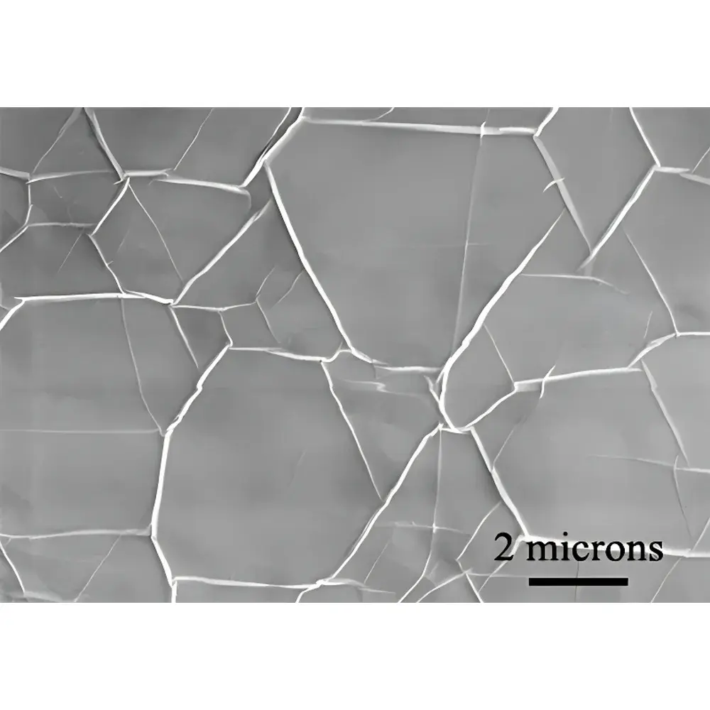
- Continuous film morphology across Ni grain boundaries and step edges, confirmed by scanning electron microscopy (SEM) and atomic force microscopy (AFM)
- Standard format: 2-inch × 2-inch (50.8 mm × 50.8 mm) sheet, compatible with standard wafer-handling tools and vacuum transfer chambers
- No polymer residue after optional thermal annealing; suitable for direct metal contact integration or dry-transfer protocols
- Batch-to-batch consistency validated via Raman I2D/IG ratio (>1.8) and full-width-at-half-maximum (FWHM) of G-band (<25 cm−1)
Sample Compatibility & Compliance
The Ni-based graphene substrate is designed for use in controlled laboratory environments including gloveboxes (O2 < 0.1 ppm, H2O < 0.1 ppm), high-vacuum chambers (base pressure ≤1×10⁻⁷ mbar), and inert-atmosphere furnaces. It complies with standard cleanroom handling protocols (Class 100–1000). While not certified to ISO 9001 or ASTM E2926 for production-grade quality assurance, each lot undergoes in-house verification per internal technical specification KS-GRA-Ni-01, which includes Raman mapping (532 nm excitation, 1 µm step size), SEM imaging at 5 kV, and sheet resistance measurement via four-point probe (typical range: 250–450 Ω/sq before transfer). Documentation includes lot-specific test reports traceable to NIST-traceable calibration standards.
Software & Data Management
As a passive material substrate, this graphene-on-nickel product does not include embedded electronics or firmware. However, it is fully compatible with industry-standard analytical platforms: Raman spectrometers (e.g., Horiba LabRAM HR Evolution, Renishaw inVia), SEM systems (Thermo Fisher Scientific Phenom, Zeiss Sigma), and electrical characterization suites (Keysight B1500A, Keithley 4200-SCS). Raw spectral and image data generated during characterization may be archived and managed under GLP-compliant workflows using LabArchives ELN or Thermo Fisher SampleManager LIMS. For regulatory submissions requiring audit trails, metadata (including lot number, date of receipt, and instrument ID) must be manually logged per 21 CFR Part 11 guidelines when used in FDA-regulated preclinical material evaluation.
Applications
- Model system for studying graphene–metal interfacial charge transfer kinetics via XPS and UPS
- Template for selective etching and transfer-free device fabrication (e.g., Ni-assisted catalytic patterning)
- Reference substrate for calibrating graphene thickness quantification methods (e.g., optical contrast, ellipsometry, EELS)
- Electrode platform for electrochemical sensors and battery anode studies (Ni acts as current collector and sacrificial layer)
- Base material for van der Waals heterostructure assembly via deterministic stacking (e.g., graphene/h-BN/MoS2)
- Fundamental investigation of strain engineering effects induced by Ni thermal expansion mismatch during cooldown
FAQ
Is the graphene film transferable to other substrates?
Yes—the film can be transferred using standard wet-etching techniques (e.g., FeCl3 or ammonium persulfate etchants) followed by PMMA-assisted pickup. Transfer yield exceeds 92% for SiO2/Si and quartz substrates.
What is the typical sheet resistance of the as-received film?
Measured via four-point probe at room temperature: 250–450 Ω/sq, depending on local defect density and Ni surface oxidation state.
Can this material be used in ultra-high vacuum (UHV) systems?
Yes—bake-out compatible up to 300 °C under UHV conditions; outgassing rate <1×10⁻⁹ mbar·L/s·cm² after 12 h at 200 °C.
Do you provide Raman spectra or SEM images for each lot?
Yes—a representative Raman map and top-down SEM micrograph are included in the Certificate of Analysis (CoA) for every shipped lot.
Is the nickel foil substrate compatible with focused ion beam (FIB) milling?
Yes—Ni exhibits low redeposition and minimal Ga implantation artifacts under 30 kV Ga+ beam conditions, enabling precise cross-section preparation for TEM lamella extraction.