GaAs Crystal Substrate Wafers for QCM and Thin-Film Deposition Applications
| Brand | Hefei Kejing |
|---|---|
| Origin | Anhui, China |
| Manufacturer Type | Authorized Distributor |
| Country of Origin | PRC |
| Model | GaAs (Undoped & Doped) |
| Pricing | Available Upon Request |
| Crystal Structure | Zincblende |
| Orientation | <100> Standard |
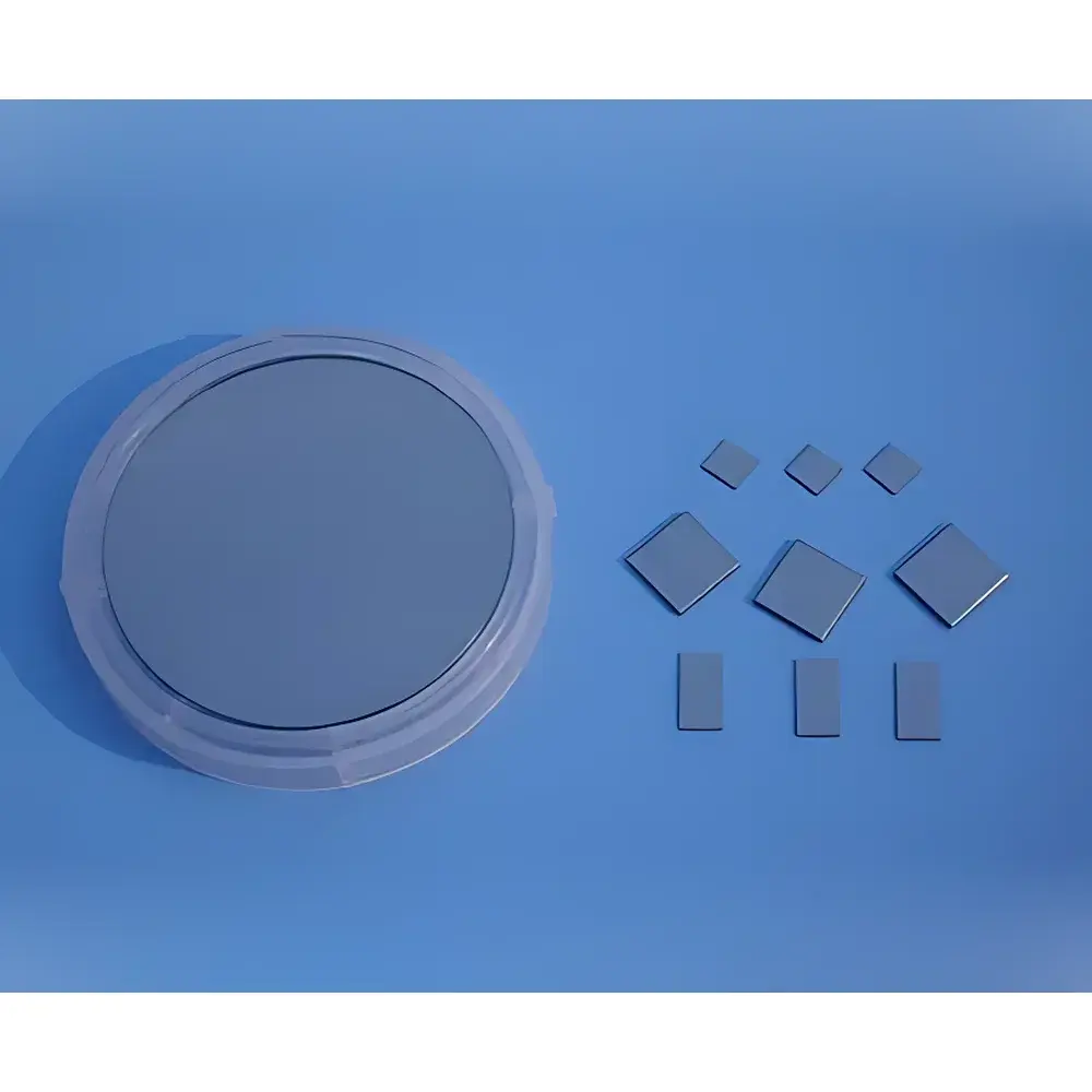
| Dimensions | 10 × 10 × 0.5 mm, Ø2″ × 0.5 mm |
| Surface Finish | Single- or Double-Side Polished |
| Surface Roughness (Ra) | <0.15 nm |
| Dislocation Density | <5 × 10⁵ cm⁻² |
| Growth Method | Liquid Encapsulated Czochralski (LEC) & Horizontal Bridgman (HB) |
| Doping Types | Undoped, Si (n-type), Cr (semi-insulating), Te (n-type), Zn (p-type) |
| Carrier Concentration Range | 5 × 10¹⁷ – >5 × 10¹⁸ cm⁻³ |
| Cleanroom Packaging | Class 1000 Cleanroom Processed, Sealed in Class 100 Cleanroom Bags |
Overview
GaAs crystal substrates are single-crystal wafers engineered for high-precision applications in electrochemical sensing, quartz crystal microbalance (QCM) transducer development, epitaxial thin-film growth (e.g., MBE, MOCVD), and optoelectronic device fabrication. Unlike silicon or quartz, gallium arsenide offers a direct bandgap (~1.42 eV at 300 K), high electron mobility (>8,000 cm²/V·s), and excellent piezoelectric coupling—making it uniquely suitable for resonant mass-sensing platforms requiring substrate-level acoustic impedance matching and low intrinsic damping. These substrates serve as foundational platforms for fabricating QCM electrodes with tailored surface chemistry, enabling real-time, label-free detection of molecular adsorption kinetics in liquid or gas phases. Their lattice-matched compatibility with III–V compound semiconductors further supports heteroepitaxial integration in advanced sensor architectures.
Key Features
- Zincblende crystal structure with controlled stoichiometry and minimal native defect density
- Available in both undoped and precisely doped variants (Si, Te, Zn, Cr) to support n-type, p-type, or semi-insulating operational requirements
- Standard orientation optimized for uniform epitaxial layer nucleation and consistent QCM resonance mode distribution
- Double-side polished wafers with Ra < 0.15 nm ensure reproducible electrode deposition and minimize interfacial scattering losses
- Dislocation density maintained below 5 × 10⁵ cm⁻²—critical for sustaining mechanical integrity during repeated QCM oscillation cycles and thermal cycling in RTP environments
- Manufactured and inspected in ISO Class 6 (1000) cleanroom facilities; final packaging performed under ISO Class 5 (100) laminar flow conditions to prevent particulate contamination
Sample Compatibility & Compliance
These GaAs substrates are compatible with standard QCM electrode metallization processes—including Au, Pt, and Al sputtering—as well as lift-off patterning for interdigitated or circular electrode geometries. Surface termination (native oxide vs. HF-last etch) can be specified to align with downstream functionalization protocols (e.g., thiol SAMs for biosensing). All wafers comply with ASTM F2197–22 (Standard Specification for Gallium Arsenide Wafers for Electronic and Optoelectronic Applications) and meet baseline requirements for GLP-compliant thin-film process qualification. While not certified to ISO/IEC 17025, documentation packages include full lot traceability, XRD rocking curve FWHM data, and four-point probe sheet resistance reports where applicable.
Software & Data Management
When integrated into QCM systems (e.g., Q-Sense E4, Stanford Research SR780, or custom lock-in amplifier setups), GaAs substrates enable high-fidelity frequency shift (Δf) and dissipation (ΔD) measurements across the 5–30 MHz fundamental range. Raw resonance data is captured via time-stamped ASCII or HDF5 exports, supporting post-acquisition analysis in MATLAB, Python (SciPy, NumPy), or commercial tools such as QTools or SAWStudio. For GMP-regulated environments, instrument control software must implement audit-trail functionality per FDA 21 CFR Part 11—though substrate-level compliance rests with the end-user’s system validation protocol.
Applications
- Resonant mass sensors for real-time monitoring of protein adsorption, polymer film swelling, and corrosion inhibitor binding on semiconductor interfaces
- Template substrates for atomic-layer epitaxy of InGaAs or AlGaAs layers in hybrid QCM–photonic integrated devices
- Reference standards in inter-laboratory round-robin studies assessing QCM sensitivity to surface roughness and acoustic loading effects
- Platform for developing chemiresistive or Schottky-barrier-based gas sensors leveraging GaAs surface state modulation
- Calibration-grade wafers in rapid thermal processing (RTP) system qualification, where thermal expansion coefficient (5.73 × 10⁻⁶ /K) and thermal conductivity (55 W/m·K) influence temperature uniformity mapping
FAQ
Are these GaAs substrates suitable for aqueous QCM measurements?
Yes—when coated with inert electrode metals (e.g., 100 nm Au) and passivated with self-assembled monolayers, they demonstrate stable resonance in buffered saline solutions over 72-hour continuous operation.
Can I specify off-axis orientations such as A or ?
Yes—custom orientations are available upon request; lead time increases by 4–6 weeks due to boule reorientation and secondary wafer slicing.
What is the typical total thickness variation (TTV) for the 0.5 mm thick wafers?
Standard TTV is ≤ 1.5 µm across 10 × 10 mm samples, measured via non-contact optical profilometry per SEMI MF1530.
Do you provide certificates of conformance or material test reports?
Yes—each shipment includes a CoC listing batch ID, growth method, doping type, orientation, dimensions, surface finish, and packaging conditions. Extended MTRs with XRD, PL, and EPD data are available at additional cost.