Hefei Kejing Ultra-Thin Silicon Wafers for Quartz Crystal Microbalance (QCM) and Electrochemical Sensing
| Brand | Hefei Kejing |
|---|---|
| Origin | Anhui, China |
| Manufacturer Type | Authorized Distributor |
| Product Origin | Domestic (China) |
| Model | Ultra-Thin Si Wafers |
| Pricing | Available Upon Request |
| Doping Type | Boron (p-type) or Phosphorus (n-type) |
| Resistivity | 10⁻³–40 Ω·cm |
| EPD | ≤100 cm⁻² |
| Oxygen Content | ≤1.8×10¹⁸ cm⁻³ |
| Carbon Content | ≤5×10¹⁶ cm⁻³ |
| Orientation | <100>, <111>, or <110> ±0.5° |
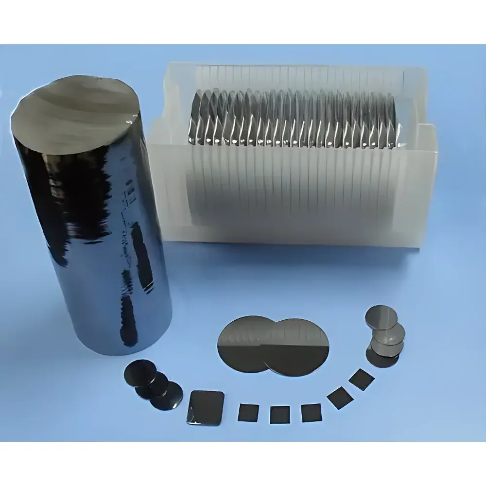
| Diameter | 2 inch (50.8 mm) |
| Thickness | 0.1 mm or 0.2 mm |
| Diameter Tolerance | ±0.4 mm |
| Thickness Tolerance | ±25 µm |
| Surface Roughness (Ra) | <10 Å |
| Optional Surface Modification | Thermal SiO₂ layer (~10–500 nm), or pre-patterned Ti/Pt metallization (Si/SiO₂/Ti/Pt stack) |
| Packaging | Individual 100-class cleanroom bags in 1000-class cleanroom environment |
Overview
Ultra-thin silicon wafers serve as high-precision substrate platforms for quartz crystal microbalance (QCM) sensor integration, electrochemical impedance spectroscopy (EIS) electrode fabrication, and surface-sensitive thin-film characterization. Engineered from Czochralski-grown monocrystalline silicon, these wafers provide atomic-level structural uniformity and exceptional thermal/chemical stability—critical for reproducible mass-loading measurements in QCM-based biosensing, corrosion monitoring, and polymer film growth kinetics. Their precisely controlled dopant profile (B or P), low defect density (EPD ≤100 cm⁻²), and ultra-low interstitial oxygen and carbon contamination ensure minimal electronic noise and long-term baseline stability under electrochemical polarization. The , , and crystallographic orientations enable orientation-dependent surface functionalization and epitaxial seeding—particularly valuable in hybrid QCM-electrode architectures where interfacial charge transfer must be decoupled from bulk semiconductor behavior.
Key Features
- Monocrystalline silicon substrates with certified crystallographic orientation (, , or ±0.5°) for consistent surface reactivity and lattice-matching in heterostructure assembly
- Ultra-thin geometries (100 µm or 200 µm thickness) optimized for mechanical compliance in resonant sensor platforms and reduced parasitic capacitance in electrochemical cells
- Surface roughness Ra <10 Å (measured by AFM), enabling uniform thin-film deposition (e.g., ALD, sputtering) and minimizing scattering-induced signal drift in optical-QCM hybrids
- Controlled resistivity range (10⁻³–40 Ω·cm) supporting both conductive and semi-insulating operational modes—essential for bias-dependent QCM-D (dissipation monitoring) and potentiostatic EIS coupling
- Optional thermally grown SiO₂ layers (10–500 nm) providing chemically inert dielectric interfaces for pH-sensitive or biomolecular recognition layers
- Pre-patterned Ti/Pt metallization (Si/SiO₂/Ti/Pt stack) available for direct integration into three-electrode electrochemical cells without additional lithography
Sample Compatibility & Compliance
These silicon wafers are compatible with standard QCM sensor holders (e.g., Q-Sense E4, Stanford Research Systems QCM200), electrochemical flow cells, and vacuum-based thin-film deposition systems. All wafers undergo final inspection and packaging in ISO Class 6 (1000-grade) cleanroom environments, sealed in ISO Class 5 (100-grade) polyethylene cleanroom bags. Batch certification includes EPD mapping, four-point probe resistivity verification, and FTIR-confirmed oxygen/carbon impurity levels—supporting GLP-compliant documentation requirements. While not certified to ASTM F1533 or SEMI standards by default, dimensional and purity specifications align with SEMI MF1530 (silicon wafer flatness) and ASTM F1250 (resistivity measurement) methodologies.
Software & Data Management
As passive substrates—not standalone instruments—these wafers integrate seamlessly with industry-standard data acquisition ecosystems: Biolin Scientific QSense software for QCM-D frequency/dissipation tracking; Gamry Framework or Metrohm Autolab NOVA for synchronized EIS/potentiodynamic control; and MATLAB/Python-based custom analysis pipelines for multi-parameter correlation (e.g., Δf vs. charge transfer resistance). Traceability is maintained via lot-specific certificates of conformance, including wafer ID, orientation, thickness, resistivity, and surface roughness—structured for import into LIMS or ELN platforms compliant with FDA 21 CFR Part 11 audit-trail requirements.
Applications
- QCM biosensor development: immobilization of antibodies, aptamers, or DNA probes on SiO₂-terminated surfaces for real-time label-free detection of analytes in serum or buffer
- Electrochemical corrosion studies: p-type Si wafers as working electrodes in chloride-containing electrolytes, correlating QCM mass loss with anodic current transients
- Thin-film polymerization monitoring: in situ QCM tracking of polymeric electrolyte growth (e.g., Nafion, PEDOT:PSS) on Ti/Pt-coated Si during electropolymerization
- Hybrid opto-electrochemical platforms: Si wafers with orientation used as substrates for plasmonic nanostructures coupled to QCM resonance for dual-mode (mass + refractive index) sensing
- Reference substrates in inter-laboratory validation studies for ASTM E2982 (standard practice for QCM calibration)
FAQ
Are these wafers suitable for high-vacuum deposition processes?
Yes—low outgassing rates and absence of organic residues (verified by XPS) make them compatible with UHV sputtering, e-beam evaporation, and MBE up to 10⁻⁹ Torr.
Can I request custom crystallographic orientations beyond //?
Yes—off-axis orientations (e.g., 4° miscut) are available upon technical review and minimum order quantity.
Do you provide wafer-level metrology reports?
Each shipment includes a certificate listing batch ID, orientation verification (XRD rocking curve FWHM), thickness profile (contact profilometry), and surface roughness map (AFM 5×5 µm scan).
Is the Ti/Pt stack deposited via DC sputtering or e-beam evaporation?
All metallized wafers use DC magnetron sputtering under Ar plasma (base pressure <5×10⁻⁷ Torr) to ensure adhesion and step coverage uniformity across 2-inch diameter.
What cleaning protocols are recommended prior to use?
We recommend standard RCA-1 (NH₄OH:H₂O₂:H₂O, 1:1:5, 75°C, 10 min) followed by HF dip (1% v/v, 30 sec) for native oxide removal—validated for retained surface roughness and dopant profile integrity.