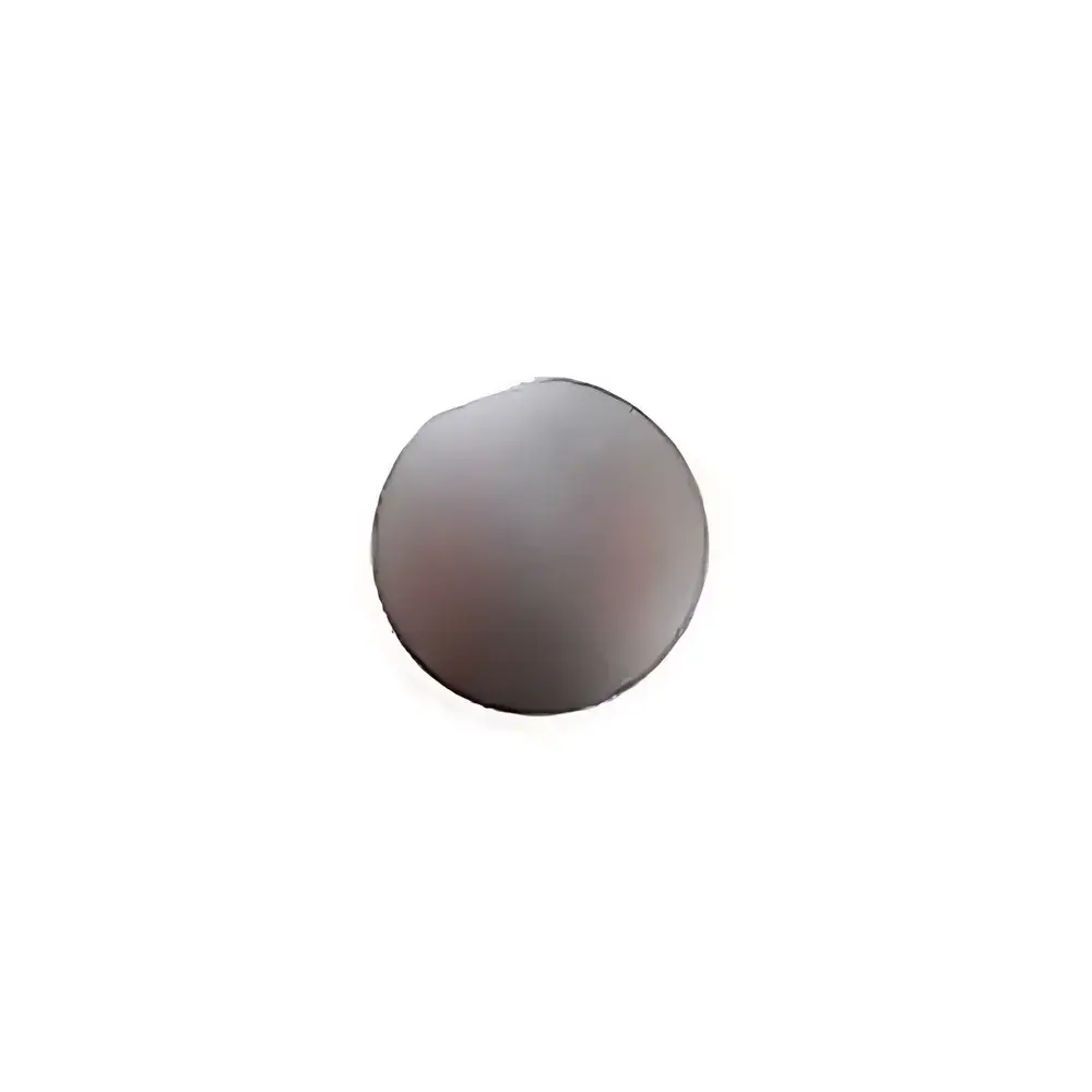
Aluminum Film on Silicon Wafer (Si Substrate) –合肥科晶 Model AF-Si-4IN
| Brand | Hefei Kejing |
|---|---|
| Origin | USA |
| Manufacturer Type | Authorized Distributor |
| Origin Category | Imported |
| Model | AF-Si-4IN (Aluminum Film on Silicon Wafer, 4-inch diameter) |
| Thickness | 3 µm |
| Resistivity | 2.65 µΩ·cm |
| Crystal Orientation | Weak (111)-oriented polycrystalline |
| Surface Roughness (Ra) | 4.87 nm (≤10 nm) |
| Si Substrate Type | N-type |
| Si Resistivity | <0.005 Ω·cm (low-doped) or 1–10 Ω·cm (standard) |
| Si Crystal Orientation | <100> ±0.5° |
| Polish | Single-side polished |
| Packaging | Vacuum-sealed in Class 100 cleanroom bags (Class 1000 cleanroom processed) or individual wafer cassettes |
Overview
The Aluminum Film on Silicon Wafer (Model AF-Si-4IN) is a precision-engineered reference and process substrate designed for semiconductor metrology, thin-film R&D, microfabrication validation, and electrical characterization applications. This product consists of a high-purity, single-side polished silicon wafer with a uniformly sputtered aluminum film deposited under controlled vacuum conditions. The Al layer exhibits weak (111)-oriented polycrystallinity—a structural signature critical for predictable adhesion behavior, electromigration resistance, and interfacial stability in back-end-of-line (BEOL) integration studies. Engineered for reproducibility and traceability, the wafer conforms to standard 4-inch (100 mm) semiconductor dimensions—diameter: 101.6 mm ±0.5 mm, thickness: 525 µm ±25 µm—with strict tolerances on crystallographic alignment ( ±0.5°) and surface finish (Ra ≤10 nm, typical 4.87 nm). Its low-resistivity N-type Si substrate (<0.005 Ω·cm or selectable 1–10 Ω·cm range) enables reliable ohmic contact formation and supports four-point probe sheet resistance mapping, Hall effect measurements, and TLM (Transfer Length Method) structure evaluation.
Key Features
- Precision 4-inch silicon substrate with tight dimensional control (±0.5 mm diameter, ±25 µm thickness)
- 3 µm thick aluminum film deposited via DC/RF magnetron sputtering—optimized for stoichiometric purity and minimal oxygen incorporation
- Consistent weak (111)-textured polycrystalline microstructure—verified by XRD and beneficial for stress management and thermal cycling reliability
- Ultra-smooth Al surface (Ra = 4.87 nm, max 10 nm)—enabling high-resolution SEM imaging, AFM topography, and lithographic patterning fidelity
- N-type silicon with controlled resistivity options: ultra-low (<0.005 Ω·cm) for grounded substrates or mid-range (1–10 Ω·cm) for device isolation studies
- Single-side polished finish meeting SEMI Standard M1–13 specifications for front-surface flatness and particle contamination
- Class 1000 cleanroom fabrication environment; final packaging in Class 100 cleanroom vacuum bags or inert-gas purged wafer cassettes
Sample Compatibility & Compliance
This aluminum-on-silicon reference wafer is compatible with industry-standard handling protocols across photolithography, etch, deposition, and analytical equipment platforms—including stepper aligners, plasma etchers (ICP/RIE), e-beam evaporators, and surface analysis tools (XPS, AES, TEM cross-sectioning). The Al film’s resistivity (2.65 µΩ·cm) aligns with bulk aluminum values per ASTM F84–22, supporting calibration of four-point probe systems per ASTM F1529. Substrate specifications comply with SEMI MF1530 (silicon wafer flatness) and SEMI MF1529 (resistivity measurement methodology). All wafers are supplied with batch-level CoC (Certificate of Conformance), including as-deposited film thickness uniformity data (±3% across diameter), surface roughness histograms, and XRD peak intensity ratios for (111)/(200) reflections. No hazardous substances are used in fabrication; RoHS 3 and REACH SVHC declarations are available upon request.
Software & Data Management
While this is a passive physical reference material—not an instrument—the associated metrological documentation supports full digital traceability. Each shipment includes a secure PDF CoC containing lot-specific QC records: film thickness (measured by spectroscopic ellipsometry), sheet resistance maps (4-point probe scan grid), and surface topography reports (AFM line scans and power spectral density analysis). Data files adhere to ASTM E2657–21 metadata standards for thin-film characterization datasets and are structured for ingestion into LIMS (Laboratory Information Management Systems) or MES (Manufacturing Execution Systems) via CSV/XML export. For GxP-regulated environments, audit trails and electronic signatures can be enabled through integration with validated document control platforms compliant with FDA 21 CFR Part 11 requirements.
Applications
- Calibration and verification of thin-film thickness measurement tools (ellipsometers, reflectometers, profilometers)
- Reference substrate for developing and qualifying Al metallization processes in MEMS, power devices, and RF IC fabrication
- Baseline material for studying interfacial diffusion, hillock formation, and electromigration kinetics under accelerated testing (JEDEC JESD22-A108)
- Substrate for depositing barrier layers (e.g., TiN, TaN) or dielectrics (SiO₂, SiNₓ) in stack integrity studies
- Electrical test vehicle for evaluating contact resistance, line resistance, and via resistance using Kelvin structures
- Teaching and training resource in university microelectronics labs for hands-on thin-film characterization exercises
FAQ
Is the aluminum film deposited via thermal evaporation or sputtering?
Sputtering—specifically DC magnetron sputtering—is used to ensure superior film density, step coverage control, and reduced columnar grain growth compared to evaporation.
Can I request custom Al thicknesses (e.g., 100 nm or 500 nm)?
Yes. Hefei Kejing offers custom thin-film configurations—including variable Al thicknesses (50 nm to 5 µm), alternative substrates (SOI, quartz, glass), and pre-patterned layouts—under NRE-supported development agreements.
Are cross-sectional TEM samples available with this wafer?
Standard wafers are not pre-thinned for TEM, but the consistent film-substrate interface quality makes them highly suitable for FIB lift-out preparation. TEM-ready sample kits (including fiducial markers and orientation guides) can be ordered separately.
What is the shelf life and recommended storage condition?
Store under dry nitrogen or argon in sealed packaging at room temperature. Unopened wafers retain specification integrity for ≥24 months. Once opened, use within 72 hours in ≤30% RH ambient to prevent native oxide growth on Al surfaces.
Do you provide ISO/IEC 17025-accredited thickness certification?
Third-party accredited thickness certification is available upon request through our partner metrology lab (ISO/IEC 17025:2017 accredited), with turnaround time of 5–7 business days post-order confirmation.


