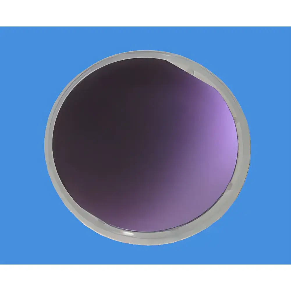
Quartz Crystal Microbalance (QCM) Substrate with Si + SiO₂ Thin-Film Coating
| Brand | Hefei Kejing |
|---|---|
| Origin | Anhui, China |
| Manufacturer Type | Authorized Distributor |
| Regional Classification | Domestic (PRC) |
| Model | Si+SiO₂ Thin-Film QCM Substrate |
| Pricing | Available Upon Request |
| Crystal Orientation | <100> or <111> |
| Doping Type | N-type or P-type |
| Fabrication Method | Dry or Wet Oxidation |
| SiO₂ Thickness | 50 nm – 1 µm (customizable) |
| Si Wafer Thickness | 0.5 mm |
| Standard Dimensions | Ø100 mm (4") or Ø50 mm (2") |
| Surface Configuration | Single-Side or Double-Side Oxidized |
| Packaging | Class 1000 Cleanroom-Processed, Sealed in Class 100 Clean Bags |
Overview
The Quartz Crystal Microbalance (QCM) Substrate with Si + SiO₂ Thin-Film Coating is a precision-engineered sensing platform designed for real-time, label-free mass detection at the nanogram level. Unlike conventional QCM sensors that rely solely on AT-cut quartz resonators, this hybrid substrate integrates a silicon wafer base with a thermally or chemically grown silicon dioxide (SiO₂) dielectric layer—enabling enhanced surface functionalization, improved thermal stability, and compatibility with standard microfabrication protocols. The device operates on the principle of piezoelectric resonance frequency shift (Δf), where mass adsorption or desorption on the SiO₂ surface induces measurable changes in the fundamental resonant frequency (typically 5–10 MHz range when coupled with appropriate quartz crystals). This configuration supports both gravimetric and viscoelastic characterization of thin-film formation, molecular binding kinetics, and interfacial hydration dynamics—particularly in electrochemical QCM-D (Quartz Crystal Microbalance with Dissipation monitoring) configurations.
Key Features
- High-purity silicon substrate available in or crystallographic orientation to accommodate epitaxial growth or anisotropic etching requirements.
- Controlled SiO₂ dielectric layer deposited via dry (thermal oxidation in O₂/H₂O ambient) or wet oxidation processes—ensuring stoichiometric SiO₂ with low defect density and uniform thickness distribution (±3 nm typical across 4″ wafers).
- Customizable oxide thickness from 50 nm to 1 µm, enabling tunable interfacial capacitance and optimized evanescent field penetration depth for QCM-based biosensing applications.
- Available in single-side or double-side oxidized configurations—supporting asymmetric surface modification strategies and reference-compensated measurement setups.
- Fabricated and packaged under ISO Class 6 (1000) cleanroom conditions; final storage in ISO Class 5 (100) clean bags ensures minimal particulate contamination (<0.1 µm particles <100 per cubic foot).
- Standard mechanical specifications: 0.5 mm thick Si wafers with polished frontside and etch-stop-ready backside—compatible with standard QCM electrode sputtering (Au, Pt, Cr/Au) and photolithographic patterning.
Sample Compatibility & Compliance
This Si+SiO₂ QCM substrate demonstrates broad compatibility with aqueous, organic, and mixed-solvent electrolytes commonly used in electrochemical impedance spectroscopy (EIS), cyclic voltammetry (CV), and QCM-D studies. The SiO₂ surface provides a stable, hydrophilic, and silanol-rich interface suitable for covalent immobilization of silane-coupling agents (e.g., APTES, GOPS), enabling robust anchoring of proteins, DNA, polymers, and nanoparticles. All substrates comply with SEMI Standard M1–0212 for silicon wafer dimensional tolerances and surface flatness (TTV < 2 µm, BOW < 10 µm). While not certified to ISO/IEC 17025, fabrication documentation—including oxidation process logs, ellipsometry verification reports, and particle count records—is retained for GLP-aligned traceability upon request.
Software & Data Management
The substrate itself is hardware-agnostic and integrates seamlessly with industry-standard QCM instrumentation platforms—including Q-Sense E4 (Biolin Scientific), Stanford Research Systems QCM200, and MaxWave QCM-D systems. When used with compliant instruments supporting FDA 21 CFR Part 11 functionality, raw frequency (Δf) and dissipation (ΔD) time-series data can be captured with full audit trail, electronic signature support, and secure user access controls. Export formats include CSV, TXT, and HDF5—enabling downstream analysis in MATLAB, Python (SciPy/NumPy), or OriginLab for Sauerbrey mass calculation, Voigt-model fitting, and hydration-corrected viscoelastic parameter extraction.
Applications
- In situ monitoring of self-assembled monolayer (SAM) formation kinetics on oxide surfaces.
- Real-time quantification of protein adsorption/desorption hysteresis under varying ionic strength or pH.
- Electrochemical deposition studies of conducting polymers (e.g., PEDOT, polyaniline) with simultaneous mass–charge correlation.
- Development of SiO₂-based QCM immunosensors targeting cardiac biomarkers (e.g., troponin I) or viral antigens (e.g., SARS-CoV-2 spike protein).
- Thin-film polymer swelling behavior in response to solvent vapor exposure—relevant to humidity sensing and smart coating development.
FAQ
Can the SiO₂ thickness be verified independently after purchase?
Yes—each batch is accompanied by ellipsometry validation data (performed at λ = 632.8 nm) and cross-sectional TEM images available upon technical inquiry.
Is the silicon substrate electrically conductive?
Conductivity depends on doping type and concentration; resistivity ranges from 0.001 Ω·cm (heavily doped N-type) to >1000 Ω·cm (light P-type); four-point probe measurements are provided in Certificate of Conformance.
Are these substrates compatible with HF-based etching steps?
Yes—the SiO₂ layer serves as a standard etch mask for KOH or TMAH bulk micromachining; HF etch rates are characterized per JIS Z 8010:2019 guidelines.
Do you offer pre-patterned electrodes on the SiO₂ surface?
Standard configurations are unmetallized; however, custom Au/Ti or Pt/Cr electrode deposition with lithographic definition (minimum line width 5 µm) is available under NRE agreement.
What is the maximum operating temperature during QCM experiments?
The Si+SiO₂ structure remains stable up to 400 °C in inert atmosphere; for electrochemical cells, recommended upper limit is 80 °C to preserve polymer coatings and electrolyte integrity.


