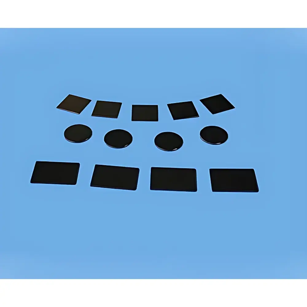
InP Crystal Substrate
| Brand | Hefei Kejing |
|---|---|
| Origin | Anhui, China |
| Manufacturer Type | Authorized Distributor |
| Origin Category | Domestic |
| Model | InP Crystal Substrate |
| Pricing | Available Upon Request |
| Crystal Structure | Single-Crystal Indium Phosphide |
| Doping | Undoped / Sn / S / Fe / Zn |
| Conductivity Type | N-type (Sn, S, Fe) / Semi-Insulating (Fe, Zn) / P-type (Zn) |
| Hardness | 3.0 Mohs |
| Density | 4.78 g/cm³ |
| Refractive Index | 3.45 (at 10.6 µm) |
| Carrier Concentration | 1–2×10¹⁶ cm⁻³ (undoped), 1–3×10¹⁸ cm⁻³ (Sn-doped), 1–4×10¹⁸ cm⁻³ (S-doped), 6–4×10¹⁸ cm⁻³ (Fe-doped) |
| Dislocation Density | <5×10⁴ cm⁻² |
| Growth Method | Liquid Encapsulated Czochralski (LEC) |
| Melting Point | 1072 °C |
| Elastic Modulus | 7.1×10¹¹ dyn·cm⁻² |
| Standard Orientations | <100> |
| Standard Dimensions | 10 mm × 10 mm × 0.5 mm |
| Surface Finish | Single-Side or Double-Side Polished |
| Surface Roughness (Ra) | <15 Å |
| Cleanroom Handling | Packaged in Class 100 cleanroom bags within Class 1000 cleanroom environment |
Overview
The InP Crystal Substrate is a high-purity, single-crystal semiconductor wafer engineered for advanced optoelectronic, photonic, and electrochemical sensing applications. Fabricated from indium phosphide (InP) via the Liquid Encapsulated Czochralski (LEC) method, this substrate exhibits exceptional crystalline integrity, low dislocation density (<5×10⁴ cm⁻²), and precise lattice matching with ternary and quaternary III–V compound semiconductors such as InGaAs, InAlAs, and InGaAsP. Its wide bandgap (1.35 eV at 300 K), high electron mobility (~5400 cm²/V·s), and direct band structure make it ideal for high-frequency transistors, laser diodes operating in the 1.3–1.55 µm telecom window, and surface acoustic wave (SAW) devices. When integrated into quartz crystal microbalance (QCM) systems—particularly those configured for electrochemical impedance spectroscopy (EIS) or mass-sensitive detection—the InP substrate serves as a robust, chemically stable electrode platform with tunable carrier concentration and surface electronic properties.
Key Features
- Single-crystal InP wafers grown by LEC method under phosphorus overpressure to suppress native defect formation
- Controlled doping profiles: undoped, N-type (Sn, S), semi-insulating (Fe, Zn), and P-type (Zn) variants available
- Standard orientation: <100>, optimized for epitaxial growth of lattice-matched heterostructures
- Surface finish options: single-side polished (SSP) or double-side polished (DSP) with Ra < 15 Å RMS roughness
- Dimensional precision: thickness tolerance ±0.05 mm; flatness ≤1 µm TTV (Total Thickness Variation)
- Class 100 cleanroom packaging: substrates sealed in static-dissipative, particle-free bags inside ISO Class 5 (Class 100) laminar flow hoods
- Traceable metrology: each lot accompanied by certified reports including XRD rocking curve FWHM, SIMS dopant depth profiling, and optical microscopy inspection
Sample Compatibility & Compliance
InP substrates are compatible with standard thin-film deposition techniques—including sputtering, thermal evaporation, MBE, and MOCVD—as well as wet chemical etching (e.g., HCl:H₃PO₄:H₂O) and dry etching (ICP-RIE using Cl₂/CH₄/Ar). The material meets ASTM F1596–22 specifications for III–V semiconductor wafers and conforms to ISO 10110–7 for optical surface quality. For regulated environments, substrates support GLP-compliant documentation workflows and can be supplied with full traceability to raw material batch, crystal pull date, and post-polish metrology records. While not inherently FDA-certified, InP wafers used in biosensor development comply with USP <1058> analytical instrument qualification protocols when deployed in validated QCM-EIS platforms.
Software & Data Management
When integrated into electrochemical QCM systems, InP substrates interface seamlessly with industry-standard data acquisition software such as NOVA (Metrohm Autolab), EC-Lab (BioLogic), or PSTrace (Princeton Applied Research). These platforms support time-resolved frequency shift (Δf) and dissipation (ΔD) monitoring, enabling real-time quantification of nanogram-level mass adsorption/desorption events. Raw sensor data is exportable in CSV or HDF5 format, supporting downstream analysis in MATLAB, Python (SciPy/Pandas), or JMP. Audit trails, user access logs, and electronic signatures align with FDA 21 CFR Part 11 requirements when deployed on validated instruments with secure network configurations.
Applications
- Epitaxial template for high-electron-mobility transistors (HEMTs) and heterojunction bipolar transistors (HBTs)
- Active layer substrate in distributed feedback (DFB) and vertical-cavity surface-emitting lasers (VCSELs)
- Electrode material in QCM-based gas sensors targeting H₂S, NH₃, and NOₓ detection
- Platform for immobilizing redox-active biomolecules in label-free electrochemical biosensing
- Reference substrate in Raman spectroscopy calibration and THz time-domain spectroscopy (THz-TDS)
- Base wafer for fabricating integrated photonic circuits operating at O-, E-, and S-band wavelengths
FAQ
What dopants are available for InP substrates, and how do they affect conductivity?
InP substrates are offered in undoped, N-type (Sn, S), semi-insulating (Fe, Zn), and P-type (Zn) configurations. Sn and S yield electron concentrations of 1–3×10¹⁸ cm⁻³ and 1–4×10¹⁸ cm⁻³ respectively; Fe-doped variants reach >6×10¹⁸ cm⁻³ with resistivity >10⁷ Ω·cm.
Can custom orientations such as <111>A or <110> be provided?
Yes—custom crystallographic orientations, off-axis cuts (±0.5°), and non-standard dimensions (e.g., 3-inch diameter, 1.0 mm thickness) are available upon request with lead times of 8–12 weeks.
Is surface passivation included, or must it be performed post-delivery?
Standard substrates are delivered with native oxide; optional sulfur-based passivation (e.g., (NH₄)₂S treatment) or dielectric capping (SiNₓ, Al₂O₃) can be applied per customer specification.
How is dislocation density verified, and what measurement standard is used?
Dislocation density is quantified via molten KOH etching followed by Nomarski differential interference contrast (DIC) microscopy, adhering to ASTM F1264–21 guidelines for etch pit density (EPD) mapping.
Are these substrates suitable for ultra-high-vacuum (UHV) MBE systems?
Yes—substrates undergo pre-bakeout at 350 °C under 1×10⁻⁶ Torr for 2 hours prior to packaging, ensuring minimal outgassing and compatibility with UHV chamber base pressures <5×10⁻¹¹ Torr.
Related Products


")