HEFEI KEJING 4-inch Si(111) Substrate with Epitaxial Aluminum Nitride (AlN) Thin Film Grown by HVPE
| Brand | HEFEI KEJING |
|---|---|
| Origin | USA |
| Manufacturer Type | Authorized Distributor |
| Origin Category | Imported |
| Model | 4-inch Si(111)/AlN Epitaxial Wafer |
| AlN Thickness | 200 nm ±10% |
| Surface Roughness (Front, as-grown) | <2 nm RMS |
| Backside Finish | As-received silicon |
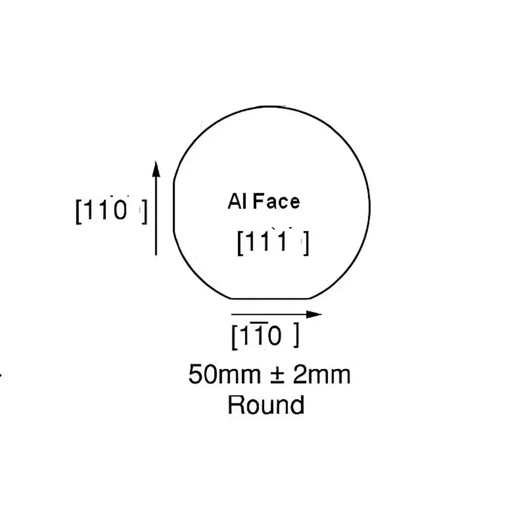
| AlN Crystal Orientation | (00.2) |
| Macrodefect Density | <10 cm⁻² |
| Substrate Material | N-type Silicon [111] |
| Diameter × Thickness | 100 mm (4 inch) × 0.5 mm |
| Resistivity | 1–10 Ω·cm |
| Surface Preparation | Single-side polished |
| Packaging | Class 1000 cleanroom environment |
Overview
The HEFEI KEJING 4-inch Si(111)/AlN epitaxial wafer is a high-purity heterostructure engineered for advanced optoelectronic, piezoelectric, and high-frequency device development. Fabricated via hydride vapor phase epitaxy (HVPE), this wafer integrates a crystalline aluminum nitride (AlN) thin film directly onto a monocrystalline silicon (111) substrate. Unlike bulk AlN substrates—cost-prohibitive and mechanically fragile—this epitaxial architecture leverages the thermal stability, scalability, and CMOS-compatibility of silicon while delivering the wide bandgap (6.2 eV), high acoustic velocity (~11,000 m/s), and strong piezoelectric coefficient (e₃₃ ≈ −2.2 C/m²) intrinsic to AlN. The (00.2)-oriented growth ensures optimal c-axis alignment for surface acoustic wave (SAW) resonators, RF filters, deep-UV photodetectors, and heterojunction transistors requiring lattice-matched, low-defect-density interfaces.
Key Features
- High-quality HVPE-grown AlN layer with controlled stoichiometry and minimal oxygen incorporation, verified by XRD rocking curve full-width at half-maximum (FWHM) < 0.3° for the (00.2) reflection
- Ultra-smooth as-grown front surface (<2 nm RMS roughness) enabling direct integration into nanoscale lithography and thin-film deposition processes without post-growth polishing
- Low macrodefect density (<10 cm⁻²), consistent with stringent requirements for high-yield microfabrication in MEMS and RF front-end modules
- N-type Si[111] substrate (1–10 Ω·cm resistivity) optimized for thermal budget compatibility during downstream processing—including metallization, etching, and passivation
- Dimensionally stable 4-inch (100 mm) format compliant with standard semiconductor handling tools and automated wafer probers
- Controlled single-side polish configuration preserves substrate backside integrity for thermal interface management and backside alignment applications
Sample Compatibility & Compliance
This wafer is compatible with industry-standard fabrication workflows including reactive ion etching (RIE), electron-beam evaporation, sputtering, and atomic layer deposition (ALD). Its structural integrity supports thermal cycling up to 600 °C in inert ambient, making it suitable for high-temperature annealing steps common in GaN-on-AlN/Si heteroepitaxy. The material system conforms to ISO 14644-1 Class 1000 cleanroom handling protocols during manufacturing and packaging. All wafers undergo non-destructive inspection per SEMI MF1390 and SEMI MF1530 standards for particle count, edge chipping, and surface contamination. Documentation includes traceable lot-level certificates of conformance covering substrate orientation, resistivity, thickness uniformity, and XRD verification of AlN c-axis alignment.
Software & Data Management
While this is a passive substrate component—not an instrument with embedded firmware—it is fully supported within mainstream semiconductor process control ecosystems. Metrology data (e.g., thickness maps from spectroscopic ellipsometry, surface topography from AFM, crystal quality from high-resolution XRD) can be imported into factory automation platforms such as Applied Materials Endura® data systems or KLA’s 3D Metrology Suite. For quality assurance and audit readiness, each wafer lot is assigned a unique identifier linked to a secure digital log containing raw characterization files, environmental exposure records (humidity/temperature during storage), and packaging validation reports—structured to align with ISO 9001:2015 documentation requirements and GLP-aligned traceability frameworks.
Applications
- High-frequency SAW and BAW resonators for 5G/6G RF front-end filtering
- Heteroepitaxial templates for GaN-based power electronics and UV-C LEDs
- Substrates for AlN-based MEMS pressure sensors and ultrasonic transducers
- Platform for studying strain relaxation mechanisms in III-nitride heterostructures
- Reference material for calibration of XRD texture analyzers and Raman spectrometers targeting wurtzite-phase nitrides
- Research-grade substrate for investigating interfacial phonon scattering and thermal boundary resistance at Si/AlN junctions
FAQ
Is this wafer suitable for direct metal lift-off patterning?
Yes—the as-grown AlN surface exhibits excellent adhesion for photoresist and compatibility with standard AZ-type resists and Ti/Al/Ni/Au metallization stacks. Pre-deposition O₂ plasma treatment is recommended to remove residual carbon and enhance metal–nitride interface bonding.
Can the backside be processed (e.g., thinning or metallization)?
The backside retains its as-received silicon morphology and is unpolished. It may be lapped, ground, or metalized using conventional backgrinding and sputtering tools—but note that thermal expansion mismatch may induce bowing if subjected to aggressive backside heating above 400 °C.
What is the typical AlN etch rate in Cl₂-based ICP-RIE?
Under standard conditions (Cl₂/BCl₃ = 20/5 sccm, 10 mTorr, 500 W ICP power), the etch rate ranges from 25–40 nm/min with selectivity >15:1 over SiO₂ hard masks.
Do you provide cross-sectional TEM samples or EBSD mapping data?
Custom characterization services—including site-specific FIB lift-out for TEM and orientation imaging via EBSD—are available upon request and subject to additional lead time and quotation.
Related Products


 and Vehicle Classification System")
