InAs Crystal Substrate (合肥科晶)
| Brand | Hefei Kejing |
|---|---|
| Origin | Anhui, China |
| Manufacturer Type | Authorized Distributor |
| Origin Category | Domestic |
| Model | InAs Crystal Substrate |
| Pricing | Available Upon Request |
| Crystal Structure | Cubic, Lattice Constant a = 5.4505 Å |
| Growth Method | Czochralski (CZ) |
| Conductivity Type | N-type |
| Doping | Undoped |
| Carrier Concentration | 2–5 × 10¹⁶ cm⁻³ |
| Electron Mobility | >18,500 cm²/V·s |
| Standard Orientations | <100>, <111> |
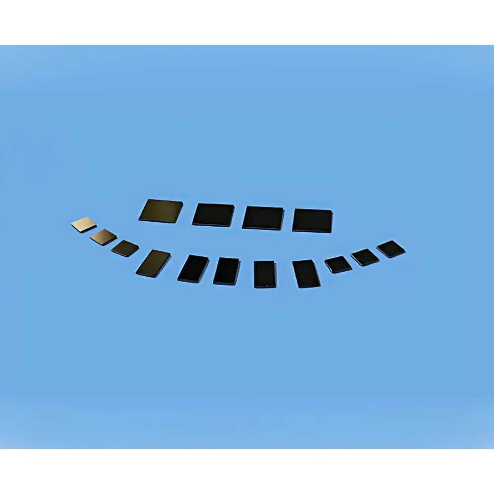
| Standard Dimensions | 10 × 10 × 0.5 mm, Ø2″ × 0.5 mm |
| Surface Finish | Single-side or double-side polished |
| Surface Roughness (Ra) | <0.15 nm |
| Cleanroom Packaging | Class 1000 cleanroom processed, sealed in Class 100 cleanroom bags |
Overview
The InAs Crystal Substrate is a high-purity, undoped indium arsenide single-crystal wafer engineered for advanced thin-film deposition, surface science investigations, and epitaxial growth applications in semiconductor research and optoelectronic device development. As a narrow-bandgap III–V compound semiconductor (Eg ≈ 0.35 eV at 300 K), InAs exhibits exceptional electron mobility and high carrier saturation velocity—making it ideal for high-frequency transistors, infrared photodetectors (3–5 µm range), quantum well heterostructures, and topological insulator studies. Grown via the Czochralski (CZ) method under controlled stoichiometric conditions, each substrate maintains structural integrity with cubic zinc-blende symmetry and lattice parameter a = 5.4505 Å. Its native N-type conductivity arises from intrinsic antisite defects (InAs) rather than intentional doping, ensuring low background impurity levels and reproducible electronic behavior across wafers.
Key Features
- High crystalline quality: Low dislocation density (<5 × 10⁴ cm⁻²) verified by X-ray rocking curve full-width at half-maximum (FWHM) < 30 arcsec
- Ultra-smooth surface finish: Ra < 0.15 nm on polished faces, compatible with molecular beam epitaxy (MBE), metalorganic chemical vapor deposition (MOCVD), and atomic layer deposition (ALD)
- Controlled orientation options: Standard and crystallographic planes available; custom off-cut angles (e.g., 2° toward [011]) supported for step-flow growth
- Dimensional flexibility: Stock sizes include 10 × 10 × 0.5 mm squares and Ø50.8 mm (2″) wafers, both with thickness tolerance ±0.05 mm
- Contamination-controlled handling: Processed in ISO Class 6 (1000) cleanroom environment; final packaging in ISO Class 5 (100) cleanroom bags with inert gas purge (N₂ or Ar)
- Traceable metrology: Each lot accompanied by certificate of analysis including orientation verification (XRD θ–2θ scan), resistivity mapping (4-point probe), and surface inspection report (optical + AFM)
Sample Compatibility & Compliance
InAs substrates are fully compatible with standard semiconductor fabrication workflows—including photolithography, lift-off, e-beam evaporation, and reactive ion etching (RIE). Their thermal expansion coefficient (5.9 × 10⁻⁶ K⁻¹) enables stable integration with common buffer layers such as AlSb and GaSb. All substrates comply with SEMI MF1390 specifications for III–V wafer geometry and surface quality. While not certified to ISO 9001 at the distributor level, material traceability aligns with GLP-compliant laboratory documentation practices. For regulated environments (e.g., academic core facilities operating under NIH or NSF instrumentation grants), batch-specific certificates support audit readiness per 21 CFR Part 11 data integrity requirements when paired with validated lab information management systems (LIMS).
Software & Data Management
Although the InAs substrate itself is a passive component, its integration into automated thin-film platforms (e.g., Kurt J. Lesker PVD systems, Veeco MBE tools) relies on standardized substrate identification protocols. Each wafer is laser-marked with a unique alphanumeric ID linked to a digital datasheet accessible via secure portal. Raw metrology data—including profilometry traces, ellipsometry spectra (n/k vs. λ), and Hall effect measurements—is delivered in CSV and HDF5 formats for interoperability with MATLAB, Python (NumPy/Pandas), and JMP statistical analysis suites. Metadata conforms to the ISA-Tab framework for reproducible materials characterization reporting.
Applications
- Epitaxial template for InAsSb, InGaAs, and InAlAs heterostructures in mid-infrared photonics
- Substrate for van der Waals heterostructure assembly in 2D material research (e.g., graphene/InAs, MoS₂/InAs interfaces)
- Platform for scanning tunneling microscopy (STM) and angle-resolved photoemission spectroscopy (ARPES) of topological surface states
- Base material for quartz crystal microbalance (QCM) electrodes requiring high-conductivity, chemically stable surfaces
- Calibration reference in terahertz time-domain spectroscopy (THz-TDS) due to predictable Drude response
- Test vehicle for novel passivation schemes (e.g., atomic-layer-deposited Al₂O₃, sulfur-based treatments) targeting surface state suppression
FAQ
What is the typical etch rate of InAs in NH₄OH:H₂O₂:H₂O (1:1:5)?
Typical isotropic etch rate is ~120 nm/min at 25 °C; rate varies with surface orientation and solution age—recommended for pre-deposition cleaning only.
Can these substrates be used directly in ultra-high vacuum (UHV) systems without outgassing concerns?
Yes; post-packaging bake-out at 150 °C for 2 h reduces residual hydrocarbons. Residual gas analysis (RGA) shows no detectable AsH₃ or InH₃ evolution below 300 °C.
Is orientation verification performed on every wafer or per-lot sampling?
Every wafer undergoes XRD θ–2θ scan at two orthogonal positions; full orientation mapping (pole figure) is available upon request for R&D qualification lots.
Do you provide substrates with pre-deposited seed layers (e.g., Ti/Au, Cr/Au)?
No—substrates are supplied bare to preserve native oxide control. Custom metallization is available through our thin-film service division under separate NDA agreement.