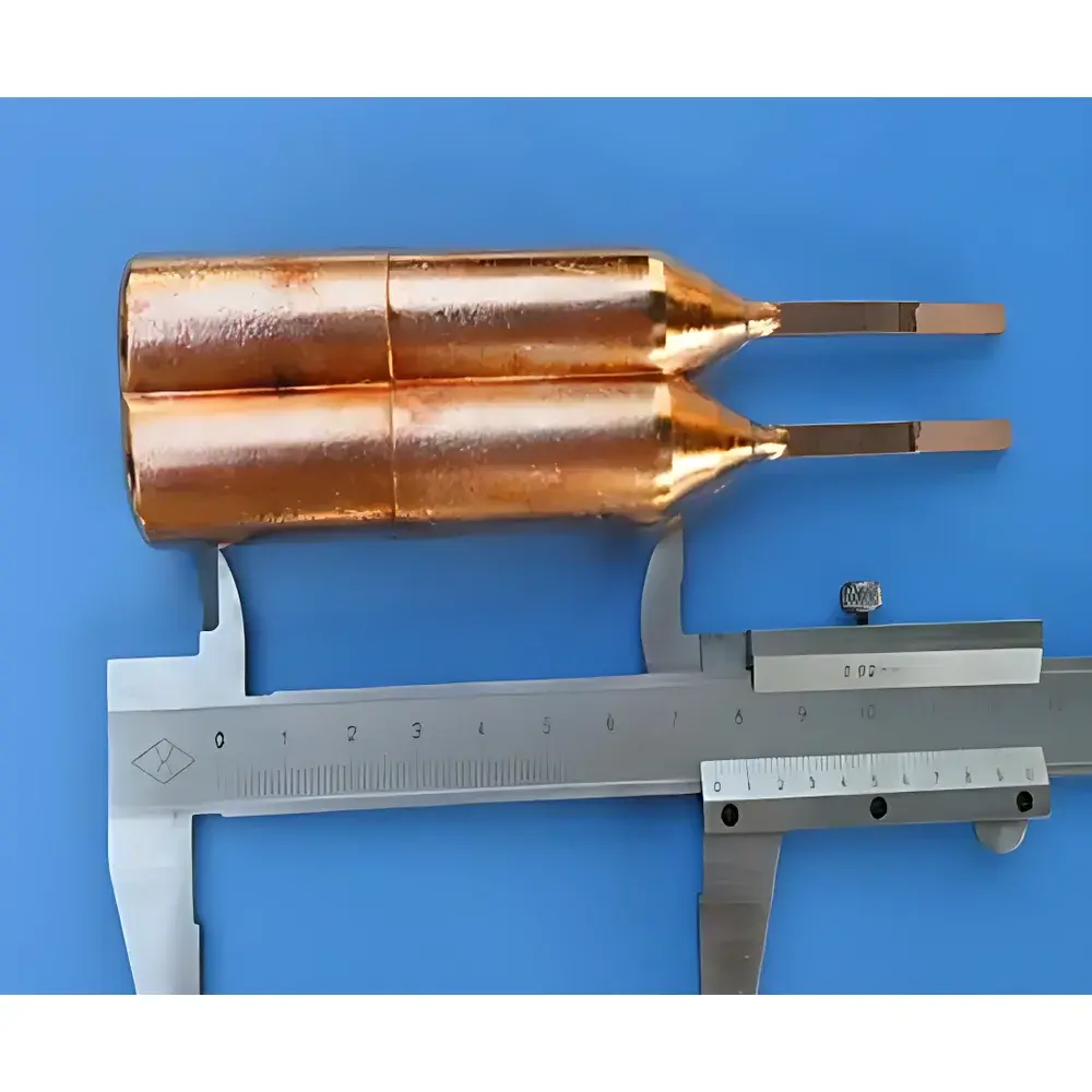
Cu Double Crystal Monochromator Substrate
| Brand | Hefei Kejing |
|---|---|
| Origin | Anhui, China |
| Manufacturer Type | Authorized Distributor |
| Country of Origin | China |
| Model | Cu Double Crystal |
| Pricing | Available Upon Request |
| Crystal Orientation | (100) at 29° and (110) at 14.5° |
| Dimensions | 10 × 10 × 1.5 mm or 10 × 5 × 1.5 mm |
| Packaging | Vacuum-sealed in 100-class cleanroom bags with aluminum foil wrapping inside 1000-class cleanroom environment |
| Storage Requirement | Store under vacuum |
Overview
The Cu Double Crystal Monochromator Substrate is a precision-engineered single-crystal component designed for use in high-resolution X-ray diffraction (XRD), synchrotron beamline monochromators, and laboratory-scale crystallographic instrumentation. Fabricated from high-purity copper (99.999% Cu), this substrate consists of two precisely oriented crystalline domains—(100) plane at Bragg angle 29° and (110) plane at 14.5°—enabling dual-wavelength selection or harmonic rejection in monochromatic X-ray systems. Its lattice-matched orientation and low dislocation density ensure minimal angular spread and high diffraction efficiency across Cu Kα (λ = 1.5418 Å) and related characteristic radiation lines. The substrate serves not as an end-user instrument but as a critical optomechanical element integrated into monochromator assemblies, goniometers, and custom diffractometer stages.
Key Features
- High-purity oxygen-free copper (OFHC) base material with verified crystallographic integrity and trace-metal certification
- Dual-orientation configuration: (100) surface normal aligned for 29° Bragg reflection and (110) surface normal for 14.5° reflection—both referenced to standard Cu Kα wavelength
- Controlled thickness tolerance of ±0.05 mm and surface flatness ≤ λ/10 over aperture (verified by optical interferometry)
- Polished to mirror finish (Ra < 0.5 nm) on active diffraction faces, with chemical-mechanical polishing (CMP) followed by in-situ hydrogen annealing to minimize surface oxide nucleation
- Strict handling protocol compliance: processed and packaged exclusively in ISO Class 6 (1000-grade) cleanrooms, sealed in ISO Class 5 (100-grade) laminar-flow bags with vacuum desiccation
Sample Compatibility & Compliance
This Cu double crystal substrate is compatible with standard UHV-compatible monochromator holders (e.g., Huber 410/420 series, Anton Paar XRK 900 stages) and integrates seamlessly into both rotating-anode and synchrotron X-ray sources. It meets dimensional and thermal expansion requirements per ASTM E975-22 (Standard Practice for X-Ray Diffraction Measurements on Metal and Alloy Specimens) for reference crystal substrates. While not a finished analytical instrument, its fabrication adheres to ISO 9001:2015-certified quality control workflows—including batch traceability, lattice parameter verification via Laue back-reflection, and post-polish surface oxide thickness quantification using XPS (≤0.3 nm native oxide layer pre-packaging). For GLP/GMP-regulated environments, full material certification (CoC), elemental analysis reports (ICP-MS), and cleanroom processing logs are available upon order confirmation.
Software & Data Management
As a passive monochromator component, the Cu Double Crystal Substrate does not incorporate embedded electronics or firmware. However, it is fully interoperable with industry-standard XRD control platforms including PANalytical HighScore Plus, Bruker DIFFRAC.SUITE, and Rigaku SmartLab Studio II. Users may import its exact lattice parameters (a = 3.615 Å, cubic Fm3m space group), orientation matrix, and thermal expansion coefficient (16.5 × 10⁻⁶ K⁻¹) directly into instrument calibration modules for automated peak position correction and rocking-curve simulation. All supplied units include a QR-coded physical label linking to downloadable technical documentation: crystallographic orientation maps, rocking-curve benchmark data (FWHM ≤ 15 arcsec at 8 keV), and vacuum storage guidelines compliant with ISO 14644-1 cleanroom packaging standards.
Applications
- X-ray monochromator assemblies requiring high-intensity, low-divergence Cu Kα output for thin-film epitaxy characterization
- Double-crystal diffractometers (DCDs) used in semiconductor wafer strain mapping and lattice mismatch analysis
- Reference standards in inter-laboratory round-robin studies coordinated under IUCr Commission on Powder Diffraction protocols
- Custom-designed beam conditioning optics for time-resolved XRD experiments at third-generation synchrotron facilities (e.g., APS, ESRF, SPring-8)
- In-situ stress/strain monitoring setups where thermal stability and minimal lattice distortion under beam load are critical
FAQ
What is the maximum allowable operating temperature for this Cu double crystal substrate?
The substrate is rated for continuous operation up to 120 °C in vacuum or inert gas environments; above this threshold, irreversible lattice relaxation may occur.
Can custom orientations or dimensions be manufactured?
Yes—Hefei Kejing supports OEM requests for non-standard Miller indices, thicknesses down to 0.8 mm, and rectangular apertures up to 15 × 20 mm, subject to minimum order quantity and extended lead time.
Is surface oxidation reversible after exposure?
No—native Cu₂O formation degrades diffraction efficiency irreversibly; therefore, strict adherence to vacuum storage and glove-box handling is mandatory.
Does this product comply with RoHS or REACH directives?
Yes—certified free of restricted substances per EU Directive 2011/65/EU and Annex XVII of REACH Regulation (EC) No. 1907/2006.
How is angular alignment verified prior to shipment?
Each unit undergoes Laue diffraction imaging and rocking-curve measurement using a calibrated Cu Kα source; full angular deviation report (±0.02°) accompanies the CoC.