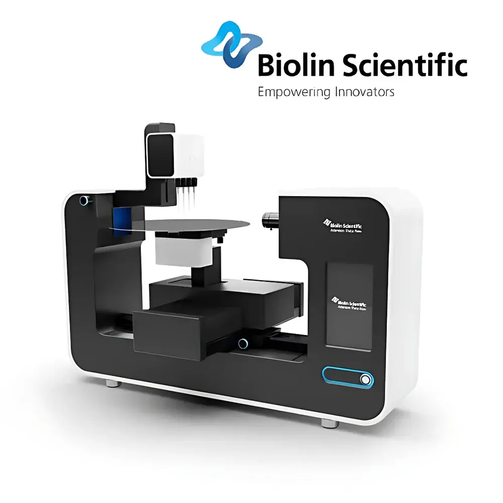
Biolin Scientific Theta Flow Wafer Video Optical Contact Angle Analyzer
| Brand | Biolin Scientific |
|---|---|
| Origin | Finland |
| Model | Theta Flow Wafer |
| Instrument Type | Benchtop Video Optical Contact Angle Analyzer |
| Contact Angle Measurement Range | Contact angle, surface tension, interfacial tension, surface free energy |
| Contact Angle Accuracy | ±0.1° |
| Sample Stage Sizes | 2", 3", 4", 5", 6", 8", 12" wafers |
| Image Resolution | 2592 × 2048 (5.3 MP) |
| Surface/Interfacial Tension Accuracy | ±0.1 mN/m (derived via pendant/sessile drop analysis) |
| Maximum Sample Diameter | 12-inch silicon wafer |
| Stage Load Capacity | 500 g |
| Automated Functions | Motorized XYZ translation + programmable rotation (0–360°), four independent software-controlled dispensers with disposable tips |
Overview
The Biolin Scientific Theta Flow Wafer is a high-precision, fully automated video optical contact angle analyzer engineered specifically for semiconductor-grade wafer metrology. It operates on the principle of sessile drop and pendant drop analysis, leveraging high-resolution imaging and advanced edge-detection algorithms to quantify interfacial interactions between liquid probes (e.g., water, diiodomethane, ethylene glycol) and solid surfaces. Designed for cleanroom-compatible integration, the system enables non-destructive, quantitative assessment of surface wettability, interfacial energetics, and heterogeneity across full-diameter wafers—up to 300 mm (12 inches). Its core measurement capabilities include static and dynamic contact angle (advancing/receding), surface free energy (via Owens-Wendt, Fowkes, or van Oss-Chaudhury-Good models), and derived surface tension/interfacial tension values. The instrument complies with ASTM D7334 (Standard Practice for Surface Wettability of Polymer Surfaces by Contact Angle Measurement) and ISO 19403-2 (Paints and varnishes — Contact angle measurements — Part 2: Determination of the surface free energy of solid surfaces), supporting traceable, repeatable surface characterization in R&D and process validation environments.
Key Features
- Fully motorized XYZ sample stage with integrated 360° programmable rotation (T340R + T340RW wafer chuck), enabling automatic radial and angular positioning across full-wafer maps.
- Four independent, software-synchronized dispensers with disposable nozzles—each individually controllable for multi-liquid surface free energy analysis without cross-contamination.
- 5.3 MP CMOS camera (2592 × 2048 resolution) with telecentric lens optics and adjustable LED backlighting for high-contrast droplet imaging under ambient or nitrogen-purged conditions.
- Vacuum-assisted wafer clamping via integrated vacuum port (ISO-KF 16 interface), ensuring sub-micron positional stability during high-speed dispensing and dynamic contact angle acquisition.
- Modular hardware architecture compliant with SEMI S2/S8 safety standards; ESD-safe construction (surface resistivity <1 × 10⁶ Ω/sq) suitable for Class 100 cleanroom deployment.
Sample Compatibility & Compliance
The Theta Flow Wafer accommodates standard semiconductor substrates—including bare Si, SiO₂, SiNₓ, SOI, GaAs, and patterned wafers—without requiring surface masking or edge trimming. Its precision alignment pins (±2.5 µm repeatability) and vacuum fixation ensure centricity within ±0.1 mm across all supported diameters (50–300 mm). The system meets ISO/IEC 17025 requirements for calibration traceability, with factory-certified verification using NIST-traceable reference liquids (water, diiodomethane, formamide). All measurement protocols support GLP/GMP documentation workflows, including electronic signatures and audit trails per FDA 21 CFR Part 11 when used with OneAttension v4.0 software.
Software & Data Management
OneAttension v4.0 provides a validated, role-based interface for method development, batch processing, and statistical reporting. Key modules include: (i) Batch Mode for sequential measurement across wafer lots (e.g., 25-point radial grid per wafer); (ii) Dynamic Contact Angle Mode with automated dispensing cycles (0.1–10 µL steps, ±0.5% volumetric accuracy); (iii) Surface Free Energy Mapping with pixel-level energy distribution visualization; (iv) Export-ready reports compliant with ASTM E2916 (Standard Guide for Validation of Software Used in Computational Chemistry) and ISO 10012 (Measurement management systems). Raw image data, metadata, and calculation logs are stored in vendor-neutral HDF5 format, supporting third-party integration via Python API.
Applications
- Plasma treatment verification: Quantifying hydrophilicity recovery post-O₂/Ar plasma exposure to validate cleaning efficacy.
- Photoresist adhesion screening: Correlating contact angle hysteresis with delamination risk in lithography stacks.
- Atomic layer deposition (ALD) precursor compatibility: Assessing surface energy evolution across ALD cycles to optimize nucleation uniformity.
- Wafer-level bonding interface analysis: Measuring interfacial tension between Si and glass substrates prior to anodic bonding.
- Post-CMP residue detection: Identifying localized hydrophobic contamination via contact angle deviation maps (±0.3° sensitivity).
FAQ
What wafer sizes does the Theta Flow Wafer support?
It supports standard semiconductor wafers from 2-inch (50 mm) to 12-inch (300 mm) diameter, with dedicated chucks and alignment fixtures for each size.
Can the system perform advancing and receding contact angle measurements automatically?
Yes—via continuous dosing and retraction cycles controlled by the four dispensers, with real-time edge detection and baseline correction.
Is the software compliant with regulatory data integrity requirements?
OneAttension v4.0 supports 21 CFR Part 11 compliance, including electronic signatures, audit trails, and user access controls when deployed on validated Windows OS platforms.
How is wafer flatness compensated during measurement?
The motorized Z-axis auto-focus routine performs real-time focal plane optimization across each measurement point, correcting for global bow and local topography up to ±20 µm.
Does the system require external vacuum or compressed air?
Only vacuum is required for wafer clamping (standard lab vacuum source, ≥−80 kPa); no compressed air or gas supply is needed for core operation.


