Fastmicro FM-W-PDS Wafer Surface Particle Detection System
| Brand | Fastmicro |
|---|---|
| Origin | Netherlands |
| Model | FM-W-PDS |
| Instrument Type | Optical Particle Counter |
| Field of View (FOV) | 4–12 inch diameter |
| Detection Principle | Dark-Field Microscopy with High-Resolution Digital Imaging |
| Minimum Detectable Particle Size | ≥0.1 µm |
| Configuration | Manual or Automated Wafer Handling |
| Dual-Side Scanning | Optional |
| Measurement Mode | Static FOV Imaging (No Sample Translation During Acquisition) |
| Compliance | Designed for ISO 14644 Cleanroom Environments, Compatible with SEMI Standards for Wafer Inspection |
Overview
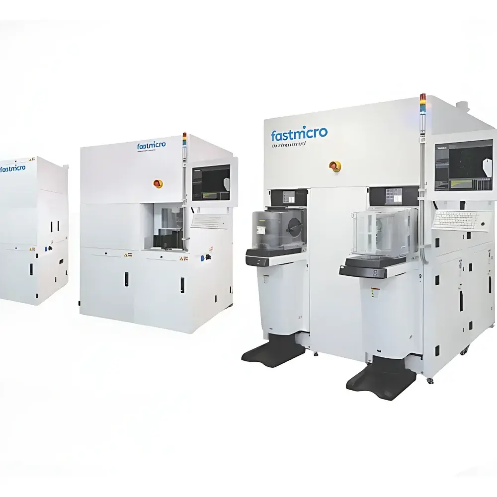
The Fastmicro FM-W-PDS Wafer Surface Particle Detection System is an engineered optical inspection platform designed for rapid, non-contact quantification of surface-borne particulate contamination on planar substrates. It operates on the principle of high-magnification dark-field microscopy coupled with calibrated monochrome CMOS imaging and sub-pixel centroid-based particle localization algorithms. Unlike conventional scanning laser or airflow-based particle counters, the FM-W-PDS captures full-field static images—eliminating mechanical translation during acquisition—which ensures measurement repeatability, reduces vibration-induced artifacts, and enables true snapshot metrology of wafer-scale surfaces. The system is purpose-built for semiconductor front-end and back-end processes, including silicon, compound semiconductor (e.g., GaN, SiC), and advanced packaging substrates such as fan-out wafer-level packaging (FOWLP) and interposer wafers. Its architecture supports integration into Class 1–10 cleanrooms and aligns with industry-standard contamination control frameworks defined by SEMI F21, ISO 14644-1, and JEDEC JESD22-A123.
Key Features
- Static field-of-view imaging: No sample motion during image capture—ensures spatial fidelity and eliminates stage-induced blur or registration drift.
- Scalable optical FOV: Configurable from 4-inch to 12-inch diameter coverage, accommodating legacy and next-generation substrate formats without hardware reconfiguration.
- Sub-0.1 µm sensitivity: Optimized illumination geometry and noise-suppressed image processing enable reliable detection and sizing of particles ≥0.1 µm in equivalent spherical diameter (ESD).
- Dual-side inspection capability (optional): Simultaneous top/bottom surface analysis via integrated dual-optic path and synchronized z-axis focus stacking.
- Modular automation interface: Standardized I/O (RS-232, Ethernet/IP, SECS/GEM) for seamless integration with factory host systems, MES, and automated material handling equipment (AMHE).
- Low total cost of ownership: Solid-state optics, maintenance-free LED illumination, and software-upgradable functionality minimize downtime and service dependency.
Sample Compatibility & Compliance
The FM-W-PDS accommodates bare and patterned wafers (Si, SOI, GaAs, sapphire, quartz), photomasks, flat panel display (FPD) glass substrates, and ceramic carriers used in advanced packaging. It supports standard wafer thicknesses (50–1000 µm) and edge profiles compliant with SEMI MW108. All optical components meet RoHS and REACH requirements. The system’s measurement traceability is established through NIST-traceable particle reference standards (e.g., Duke Scientific latex spheres, ISO 21501-4 certified). Data integrity conforms to FDA 21 CFR Part 11 requirements when deployed with optional audit trail and electronic signature modules. Routine verification follows ASTM E2587 for particle counting statistics and ISO 21501-4 for instrument calibration validation.
Software & Data Management
Control and analysis are executed via Fastmicro VisionSuite™ v4.x—a Windows-based application supporting multi-user role permissions, SOP-driven workflows, and configurable pass/fail thresholds per defect class (e.g., metallic vs. dielectric, clustered vs. isolated). Raw image data is stored in TIFF-6.0 format with embedded metadata (timestamp, lens ID, exposure settings, calibration checksum). Quantitative outputs include particle count per size bin (0.1–10 µm, logarithmic bins), spatial density maps (particles/cm²), centroid coordinates (X/Y in mm), and ISO-class-compliant cleanliness reports. Export formats include CSV, XML (SEMI E54), and PDF-certified reports with digital signatures. Integration with LIMS and SPC platforms is supported via ODBC and RESTful API endpoints.
Applications
- Pre- and post-lithography particle monitoring on 200 mm / 300 mm / 450 mm wafers
- Contamination screening of EUV mask blanks and pellicles
- Post-CMP residue verification in copper/low-k interconnect processes
- Wafer-level reliability qualification for MEMS, power devices, and RF ICs
- In-line cleanliness validation prior to bonding, dicing, or encapsulation steps
- OEM integration into cluster tools, wet benches, and dry etch load ports
FAQ
Does the FM-W-PDS require vacuum or inert gas purging for operation?
No—operation is performed under ambient cleanroom conditions; no vacuum chamber or purge gas interface is needed.
Can the system distinguish between particles and surface defects such as scratches or pits?
Yes—via multi-angle illumination sequencing and height-sensitive contrast analysis, enabling morphological classification beyond simple intensity thresholding.
Is remote diagnostics and firmware update supported?
Yes—Secure remote access is enabled via TLS-encrypted VNC with customer-defined firewall policies; firmware updates are delivered as signed .pkg bundles with rollback capability.
What level of training is required for operators?
Basic operation requires ≤2 hours of guided instruction; advanced metrology configuration and SPC reporting require certified Fastmicro Application Engineer support.
Is the FM-W-PDS suitable for R&D labs with low-volume, high-variability sample sets?
Yes—the manual loading variant includes adjustable focus presets, customizable ROI masking, and scriptable batch analysis for heterogeneous substrate types.


