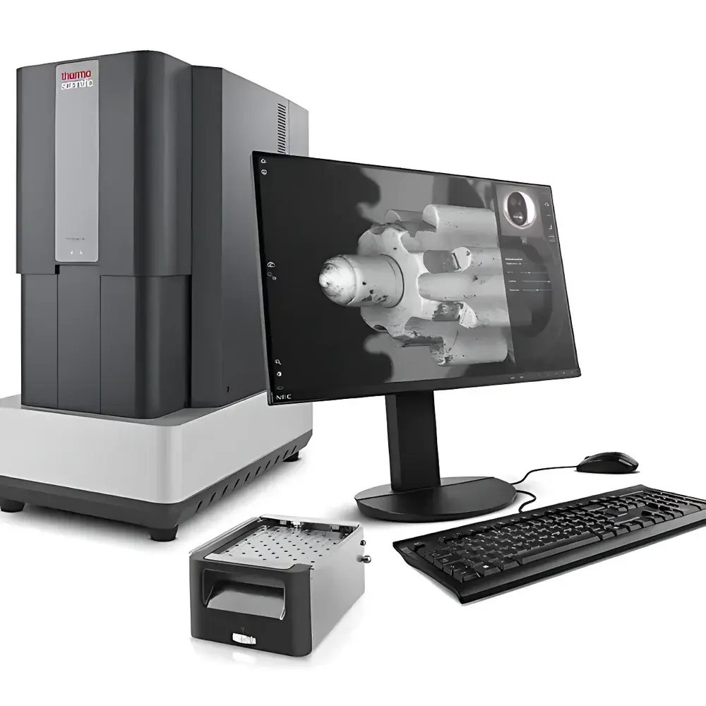
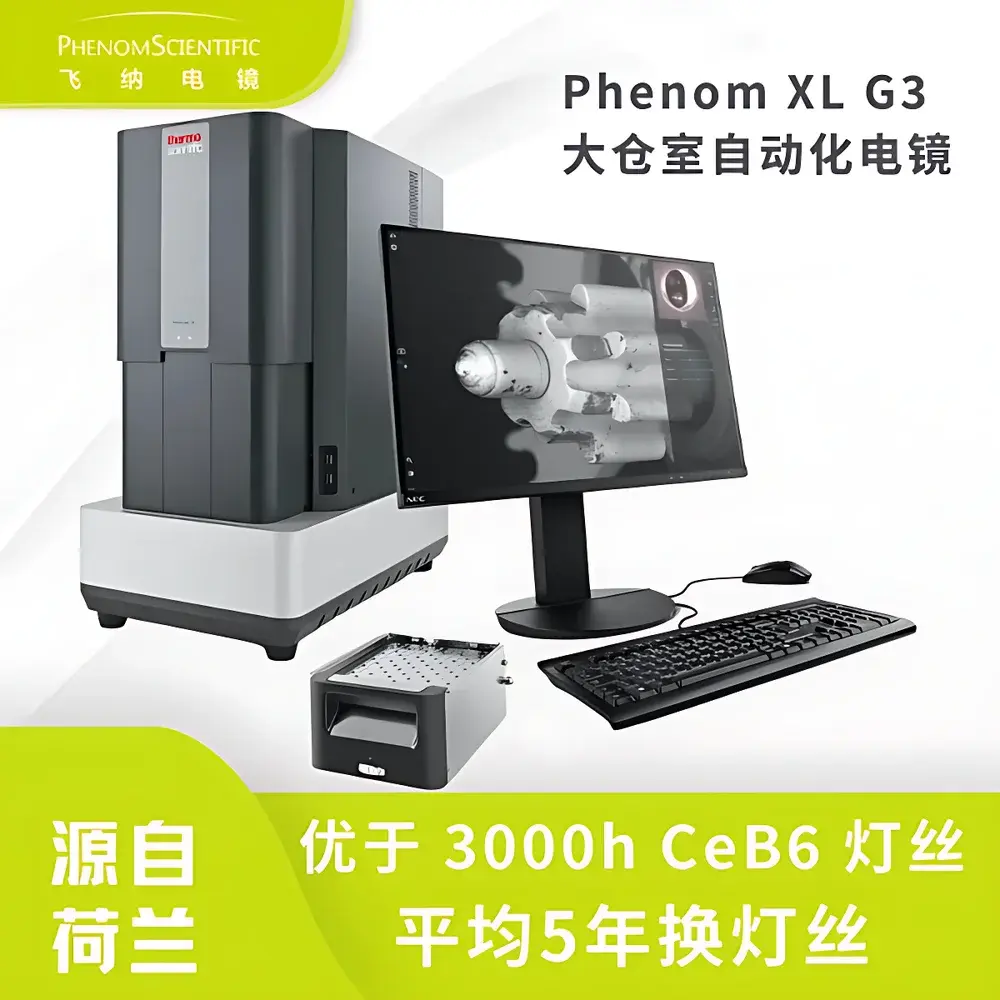
Thermo Scientific Phenom XL Desktop Scanning Electron Microscope with Large Chamber
| Key | Brand: Thermo Scientific Phenom |
|---|---|
| Origin | Netherlands |
| Model | Phenom XL |
| Instrument Type | Desktop SEM |
| Electron Source | CeB6 (Cerium Hexaboride) |
| Secondary Electron Resolution | <8 nm |
| Maximum Magnification | 200,000× |
| Accelerating Voltage Range | 4.8–20.5 kV |
| Backscattered Electron Resolution | <8 nm |
| Vacuum Modes | Low / Medium / High |
| Pump-down Time | ≤30 s |
| Standard Operating Voltages | 2, 5, 10, 15, 20 kV |
| Integrated EDS | Yes (ChemiSEM platform) |
| Stage Capacity | Up to 36 samples (automated workflow) |
| Lamp Life | ≥3000 h (CeB6) |
| Software Interface | Python Programmable Interface (PPI), ParticleMetric, FiberMetric, ChemiPhase, MAPS |
Overview
The Thermo Scientific Phenom XL Desktop Scanning Electron Microscope (SEM) is an industrial-grade, large-chamber SEM engineered for high-throughput, low-maintenance operation in non-traditional environments—including production floors, quality control laboratories on upper building levels, and even mobile or field-deployed settings. Unlike conventional floor-standing SEMs requiring dedicated vibration-isolated rooms and high-voltage infrastructure, the Phenom XL integrates a patented mechanical damping system and compact vacuum architecture, enabling stable imaging without structural modification. Its core electron optical design employs a high-brightness cerium hexaboride (CeB6) thermionic source, delivering superior signal-to-noise ratio at low accelerating voltages (down to 2 kV), essential for charge-sensitive, non-conductive, or beam-delicate specimens—such as polymers, biological tissues, ceramics, and uncoated solar cell surfaces. The instrument operates on the fundamental principle of scanning electron-sample interaction: incident electrons generate secondary electrons (SE), backscattered electrons (BSE), and characteristic X-rays, which are simultaneously collected to yield topographic, compositional, and phase information.
Key Features
- Large sample chamber accommodating specimens up to 100 mm in diameter and 50 mm in height—ideal for wafers, filters, fracture surfaces, and multi-component assemblies.
- CeB6 electron source with ≥3000 h operational lifetime, reducing filament replacement frequency to approximately once every five years under typical QC usage.
- Optimized low-kV imaging performance: enhanced BSE detector sensitivity and improved vacuum staging enable high-fidelity imaging at 2–5 kV without metal coating—critical for preserving native surface chemistry and morphology.
- Integrated ChemiSEM platform: real-time, pixel-by-pixel correlation of BSE intensity and energy-dispersive X-ray spectroscopy (EDS) data, generating quantitative elemental distribution maps in color during acquisition.
- Automated stage with programmable 36-position sample holder, supporting unattended overnight acquisition of multi-point datasets across large-area or heterogeneous samples.
- Sub-30-second pump-down time and ambient-pressure loading via airlock mechanism—eliminating lengthy vacuum cycles and maximizing instrument uptime.
- Python Programmable Interface (PPI): open API for integration with LIMS, MES, or factory automation systems, enabling full traceability and compliance with ISO/IEC 17025 and FDA 21 CFR Part 11 requirements.
Sample Compatibility & Compliance
The Phenom XL accommodates diverse material classes without mandatory conductive coating—including insulators (glass, paper, textiles), hydrated or beam-sensitive materials (freeze-dried biologicals, pharmaceutical powders), and coarse-grained composites (ceramics, battery electrodes, metallurgical cross-sections). Its low-voltage capability mitigates charging artifacts while preserving nanoscale surface detail. The system complies with IEC 61000-6-3 (EMC emissions) and IEC 61000-6-2 (immunity), and its software architecture supports audit trails, user access control, and electronic signatures per GLP/GMP and ISO 13485 frameworks. Optional EDS hardware meets ASTM E1508 and ISO 16577 standards for qualitative and semi-quantitative microanalysis.
Software & Data Management
Phenom XL ships with a unified software suite eliminating context switching between imaging and analysis modules. ParticleMetric automates particle sizing, shape classification, and statistical reporting per ISO 13322-2; FiberMetric quantifies fiber length, diameter, and orientation distributions in accordance with ASTM D3377. ChemiPhase performs phase identification and area-fraction quantification by clustering EDS spectra using multivariate statistical algorithms. MAPS enables hierarchical stitching of hundreds of high-resolution frames into gigapixel-scale mosaics—with embedded spectral metadata retained at each pixel level. All datasets are stored in vendor-neutral formats (TIFF, HDF5, .csv), ensuring long-term archival integrity and third-party interoperability.
Applications
The Phenom XL serves as a primary characterization tool in semiconductor wafer defect review, additive manufacturing powder morphology assessment, filtration media pore structure analysis, failure analysis of battery cathodes, and forensic fiber comparison. In R&D labs, it accelerates formulation screening by correlating microstructure (grain size, porosity, phase segregation) with functional performance metrics. In regulated manufacturing, its automated workflows support routine release testing of medical device coatings, catalyst substrates, and ceramic insulators—fully documented for regulatory submissions.
FAQ
Does the Phenom XL require external vibration isolation?
No—the built-in mechanical damping system allows stable operation on standard laboratory benches, production line carts, or upper-floor facilities without passive or active isolation platforms.
Can uncoated biological samples be imaged without charging artifacts?
Yes—optimized low-kV (2–5 kV) imaging combined with enhanced BSE detection enables high-contrast, artifact-free visualization of non-conductive, hydrated, or frozen-hydrated specimens.
Is EDS analysis performed in real time during SEM imaging?
Yes—ChemiSEM continuously acquires and processes EDS spectra in parallel with SE/BSE imaging, enabling live elemental mapping synchronized with morphological observation.
What is the maximum sample thickness supported in the large chamber?
The chamber accepts samples up to 50 mm in height and 100 mm in diameter, with full motorized stage travel (X/Y: ±25 mm, Z: 0–40 mm) and tilt capability (±90°) for oblique-angle imaging.
How does the system ensure data integrity for regulated environments?
Audit trail logging, role-based user permissions, electronic signatures, and encrypted raw data storage comply with FDA 21 CFR Part 11, EU Annex 11, and ISO/IEC 17025 documentation requirements.


