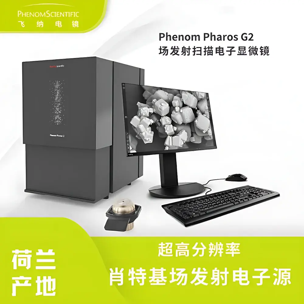
Phenom Pharos G2 Desktop Field-Emission Scanning Electron Microscope (FE-SEM)
| Brand | Phenom |
|---|---|
| Origin | Netherlands |
| Model | Phenom Pharos G2 |
| Instrument Type | Desktop/Compact FE-SEM |
| Electron Source | Schottky Field Emission Gun (FEG) |
| SEM Class | High-Resolution Field-Emission SEM |
| Secondary Electron (SE) Resolution | ≤1.5 nm |
| Backscattered Electron (BSE) Resolution | ≤1.5 nm |
| Magnification Range | 10× to 2,000,000× |
| Accelerating Voltage | 1 kV – 20 kV |
| Standard Detectors | In-lens SE Detector, Solid-State BSE Detector |
| Optional Detector | Energy-Dispersive X-ray Spectrometer (EDS) |
Overview
The Phenom Pharos G2 is a compact, high-performance field-emission scanning electron microscope engineered for research-grade nanoscale characterization in space-constrained laboratory environments. Unlike conventional thermionic or tungsten-based SEMs, the Pharos G2 integrates a high-brightness Schottky field-emission electron source—delivering superior beam coherence, current stability, and long-term emission consistency without filament replacement. Its optimized electron optical column enables sub-2 nm resolution imaging at both high and low accelerating voltages (1–20 kV), making it uniquely suited for beam-sensitive, non-conductive, and heterogeneous samples—including polymers, biological tissues, battery cathode/anode powders, thin-film semiconductors, and uncoated ceramics. The system operates under high vacuum with an integrated turbomolecular pumping station and features a fully automated vacuum lock cycle completing in under 15 seconds—eliminating the need for conductive sputter coating and enabling rapid, routine analysis across academic, industrial R&D, and quality control settings.
Key Features
- Schottky field-emission electron gun with >1,500-hour operational lifetime and <0.5% beam current drift over 8 hours
- Sub-1.5 nm resolution at 1 kV (SE mode) and 5 kV (BSE mode), verified per ISO 16700:2016 standards
- Dual-mode imaging: simultaneous acquisition of topographic (SE) and compositional (BSE) contrast with real-time signal mixing
- Integrated motorized stage with 5-axis precision control (X/Y/Z/tilt/rotation), programmable stage mapping, and automatic area stitching
- Optical navigation camera (1.3 MP color CMOS) co-registered with SEM field-of-view for intuitive sample positioning
- Self-aligning, maintenance-free electron optics—no user-accessible alignment knobs, stigmators, or aperture adjustments required
- Modular EDS integration pathway compliant with ASTM E1508 and ISO 22309 for quantitative elemental mapping and point analysis
Sample Compatibility & Compliance
The Pharos G2 accommodates specimens up to 100 mm in diameter and 40 mm in height without disassembly. Its low-voltage imaging capability (down to 1 kV) minimizes charging on insulators and reduces beam-induced damage in organic, hydrated, or nanostructured materials—supporting direct observation of as-received lithium-ion electrode particles, freeze-dried biofilms, or uncoated polymer blends. All hardware and software comply with IEC 61000-6-3 (EMC), IEC 61010-1 (safety), and meet essential requirements for CE marking. System firmware supports audit trails, electronic signatures, and user access levels aligned with GLP and ISO/IEC 17025 documentation frameworks. Optional EDS modules are validated per ASTM E456 for repeatability and certified for traceable calibration using NIST SRM reference materials.
Software & Data Management
Acquisition and analysis are managed via Phenom Desktop Software v5.x—a Windows-based platform supporting fully automated workflows including autofocus, astigmatism correction, contrast/brightness optimization, and multi-region survey imaging. Raw image data is stored in TIFF and proprietary .SEM formats with embedded metadata (kV, WD, dwell time, detector gain, stage coordinates). Batch processing tools enable batch resizing, noise reduction (non-local means filtering), and particle analysis (size, shape, distribution) per ISO 9276-2. For regulated environments, optional 21 CFR Part 11 compliance packages provide role-based permissions, electronic signature logging, and immutable audit trails. Export options include CSV (for EDS spectra), SVG (vector overlays), and standardized PDF reports with embedded spectral libraries and measurement annotations.
Applications
- Materials science: grain boundary analysis in sintered ceramics, phase distribution in metal alloys, dispersion homogeneity in nanocomposites
- Lithium-ion battery R&D: morphology evolution of NMC/LFP cathodes after cycling, SEI layer thickness estimation, dendrite detection on Li-metal anodes
- Semiconductor process control: defect classification on 300 mm wafers, trench profile metrology, contamination identification in packaging substrates
- Life sciences: ultrastructural examination of cryo-fractured tissue sections, collagen fiber orientation in decellularized scaffolds, nanoparticle internalization in fixed cells
- Failure analysis: fracture surface characterization in additively manufactured components, corrosion pit depth profiling, interfacial delamination in multilayer coatings
- Quality assurance: incoming raw material verification (e.g., pigment particle size distribution), coating thickness validation via cross-section imaging, weld seam integrity assessment
FAQ
Does the Pharos G2 require external vibration isolation?
No—the instrument incorporates 27 independent passive damping elements within its base chassis and meets ISO 20816-1 Class A vibration sensitivity thresholds. It operates reliably on standard laboratory benches without active anti-vibration tables.
Can non-conductive samples be imaged without sputter coating?
Yes—low-kV SE imaging (1–3 kV) combined with charge compensation via beam-induced gas ionization enables stable, artifact-free imaging of untreated polymers, glass, and biological specimens.
Is EDS quantification supported out of the box?
EDS is available as a factory-installed option. Quantitative analysis requires optional standards-based calibration and ZAF matrix correction algorithms, both supported in the Phenom EDS Suite v3.2.
What is the typical maintenance schedule?
The Schottky emitter requires no routine replacement for ≥1,500 hours; the turbomolecular pump oil is rated for 15,000 hours. Annual preventive maintenance includes vacuum gauge calibration and detector gain verification—typically completed onsite in <2 hours.
How does data integrity align with regulatory requirements?
With the Part 11 Compliance Module enabled, all user actions, parameter changes, and report generations are timestamped, digitally signed, and stored in an encrypted database with write-once-read-many (WORM) archival capability.


