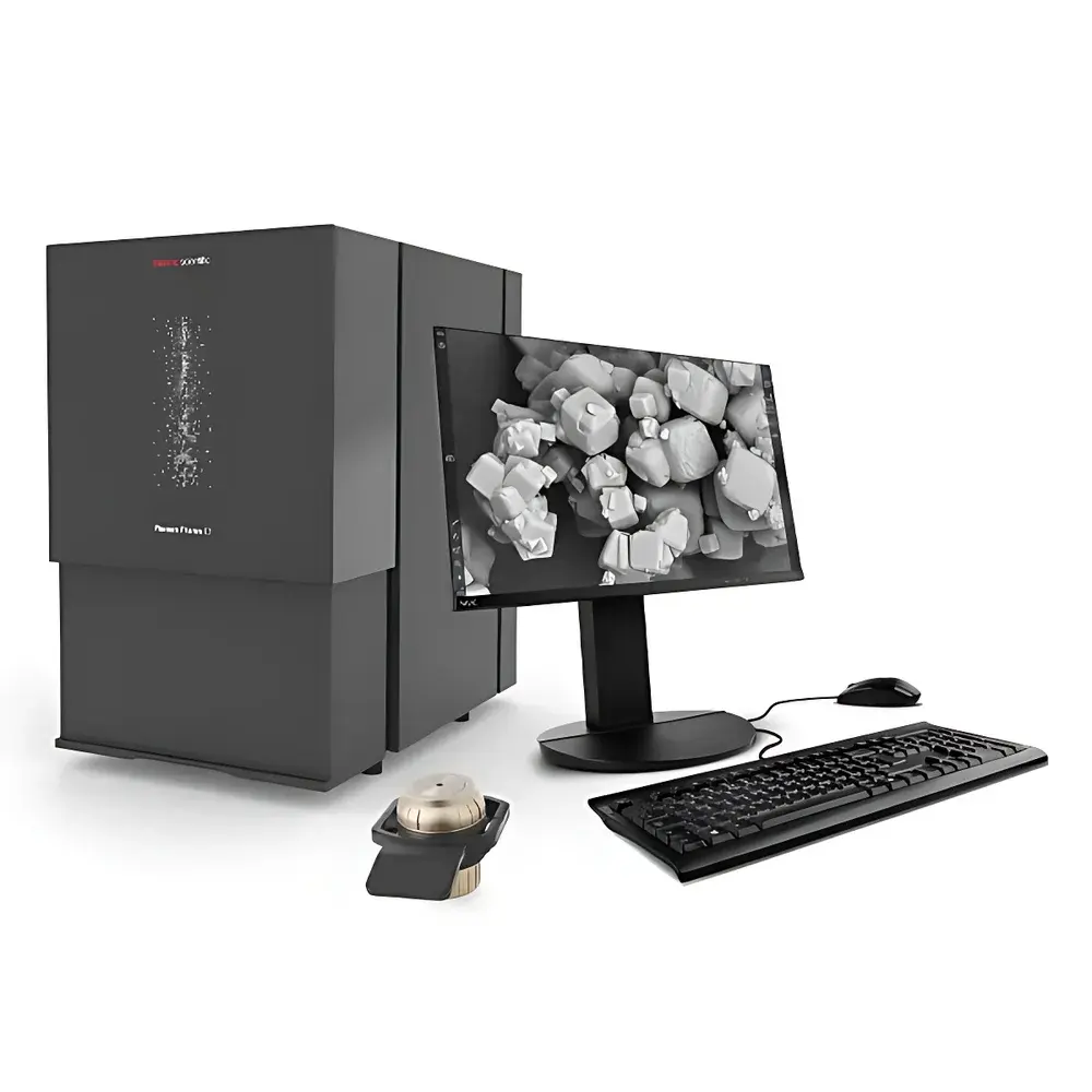
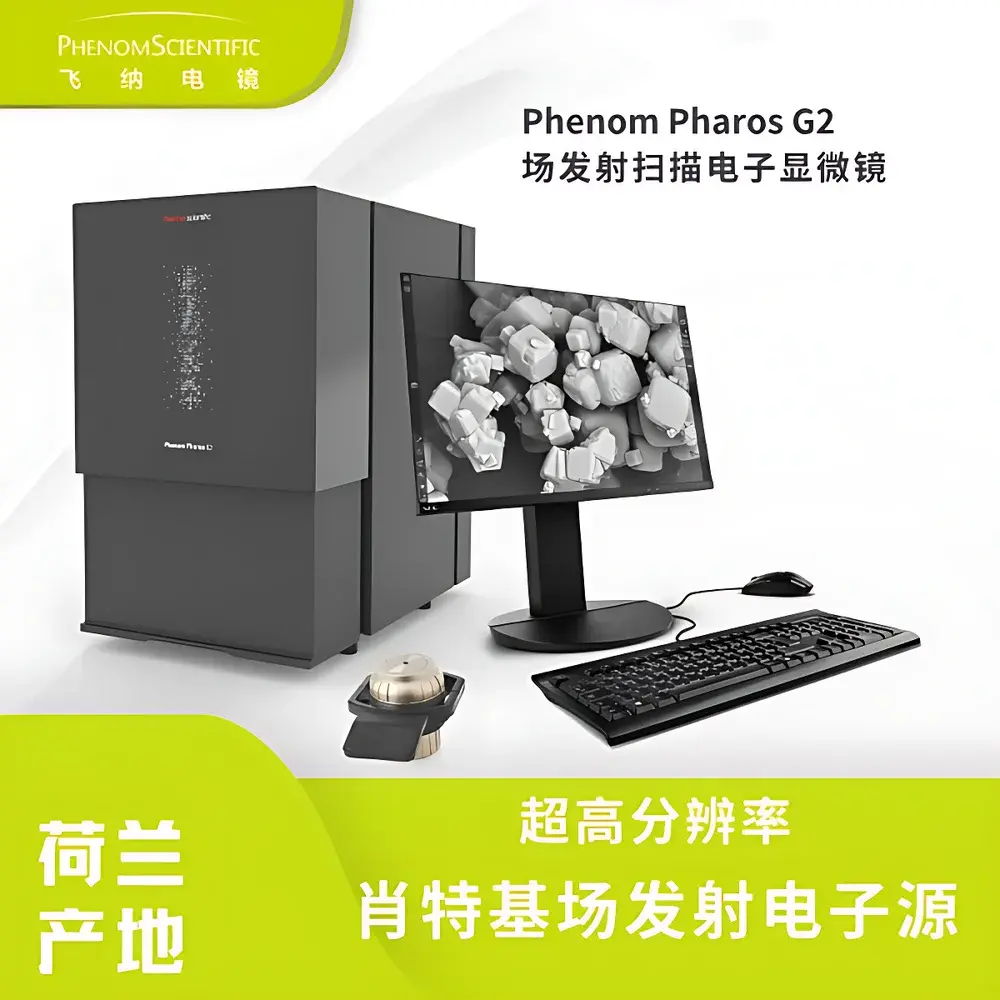
Phenom Pharos G2 Desktop Field-Emission Scanning Electron Microscope
| Brand | Phenom |
|---|---|
| Origin | Netherlands |
| Manufacturer | Phenom-World B.V. |
| Type | Desktop SEM |
| Electron Source | Schottky Field-Emission |
| Resolution (SE & BSE) | 1.5 nm |
| Maximum Magnification | 2,000,000× |
| Accelerating Voltage Range | 1–20 kV |
| Integrated EDS Capability | Yes |
| Vacuum Pumping Time | ≤15 s |
| Vibration Isolation | 27 Independent Passive Damping Units |
| Sample Stage | Motorized, Fully Automated |
| Optical Navigation | Integrated Color Optical Microscope |
| Conductive Coating Not Required | Yes |
Overview
The Phenom Pharos G2 is a second-generation desktop field-emission scanning electron microscope (FE-SEM) engineered by Phenom-World B.V. in the Netherlands. Unlike conventional thermionic or cold-field emission systems, the Pharos G2 employs a high-brightness Schottky-type thermal field-emission electron source, delivering exceptional beam stability, long source lifetime (>2,000 hours), and superior signal-to-noise ratio across its full accelerating voltage range (1–20 kV). Its compact, integrated architecture implements a fully sealed electron optical column with zero-maintenance electromagnetic lens design—eliminating routine alignment or filament replacement. The instrument operates on a robust vibration-isolation platform featuring 27 independent passive damping units, enabling stable imaging even on standard laboratory benches without external anti-vibration tables. Designed for routine high-resolution characterization in QC labs, materials science departments, and failure analysis centers, the Pharos G2 bridges the performance gap between benchtop and floor-standing FE-SEMs while maintaining compliance with ISO/IEC 17025 operational traceability requirements.
Key Features
- Sub-1.5 nm resolution imaging in both secondary electron (SE) and backscattered electron (BSE) modes—validated per ASTM E1558–21 guidelines for SEM resolution reporting
- Optimized low-kV performance (down to 1 kV) for charge-free, surface-sensitive imaging of non-conductive, beam-sensitive, or hydrated specimens without carbon/gold sputter coating
- Integrated color optical microscope with panoramic navigation—enabling rapid region-of-interest selection and seamless transition from mm-scale overview to nm-scale detail
- Fully motorized 5-axis sample stage with programmable positioning repeatability ±0.5 µm, supporting automated multi-point acquisition and tilt-series workflows
- On-board vacuum system achieving operational pressure (<1 × 10⁻⁴ Pa) in ≤15 seconds via turbomolecular pump with automatic gate valve control
- Embedded EDS detector with silicon drift technology (SDD), optimized for high-count-rate elemental mapping and quantitative analysis per ISO 14739–1 standards
- Intuitive touch-enabled software interface compliant with FDA 21 CFR Part 11 for audit trail, electronic signature, and user access control
Sample Compatibility & Compliance
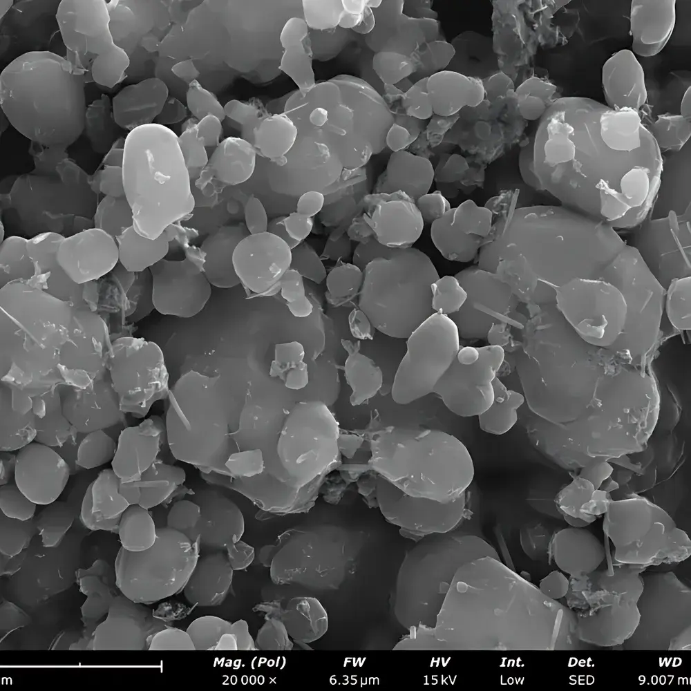
The Pharos G2 accommodates samples up to 100 mm in diameter and 50 mm in height—including bulk metals, ceramics, polymers, biological tissues, geological sections, and semiconductor wafers. Its low-voltage imaging capability minimizes charging artifacts and subsurface electron penetration, making it suitable for insulating materials such as glass fibers, pharmaceutical powders, and uncoated biological specimens. All hardware and software modules conform to CE marking directives (2014/30/EU EMC, 2014/35/EU LVD), RoHS 2011/65/EU, and IEC 61000-6-2/6-3 immunity/emission standards. The system supports GLP/GMP-aligned operation through configurable user roles, session logging, and encrypted data export protocols.
Software & Data Management
Acquisition and analysis are managed via Phenom Desktop Software v5.x—a Windows-based platform supporting real-time image stitching, particle analysis (ISO 13322-1), roughness quantification (ISO 25178), and EDS spectral deconvolution using standardless ZAF matrix correction. Raw data (TIFF, BMP, EDS spectra in .eds/.emsa formats) are stored with embedded metadata including HV, WD, dwell time, magnification, and detector geometry. The software integrates with LIMS environments via OPC UA and supports DICOM-SEM export for cross-platform archival. Remote diagnostics and firmware updates occur over TLS-encrypted connections, with optional 24/7 cloud-based health monitoring enabled via Phenom Connect.
Applications
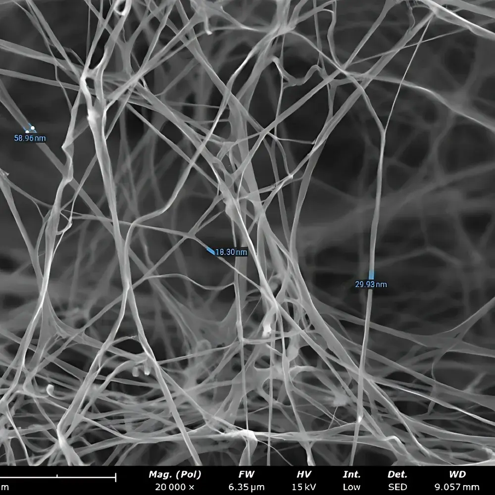
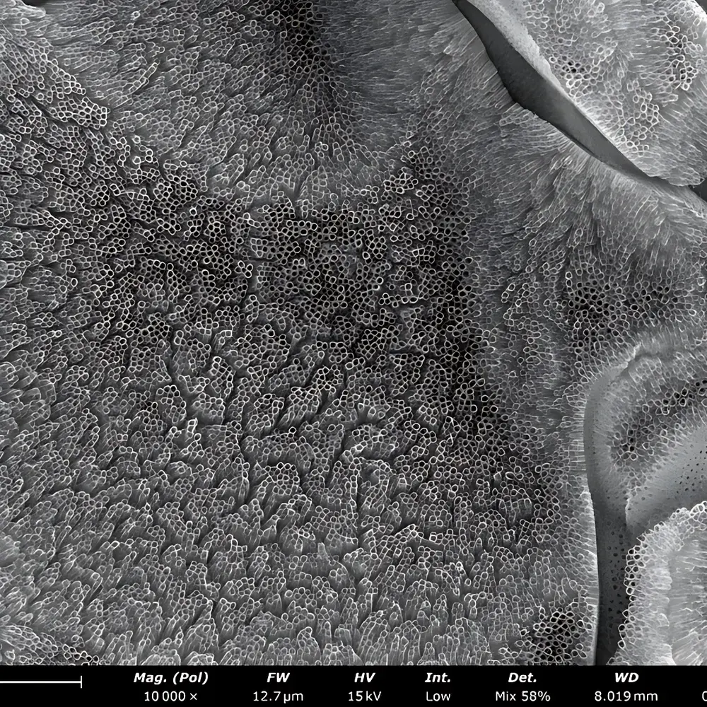
The Pharos G2 serves diverse analytical workflows: failure analysis of solder joints and PCB delamination; morphology assessment of catalyst nanoparticles and battery electrode coatings; contamination identification in cleanroom environments; fiber diameter distribution in nonwovens; pore structure quantification in filtration membranes; and forensic particulate analysis per SWGDOC guidelines. Its ability to generate high-fidelity topographic and compositional datasets without cryo-preparation or conductive coating expands applicability into life sciences (e.g., plant stomata, insect cuticle) and soft-materials research where conventional SEM preparation would induce structural artifacts.
FAQ
Does the Pharos G2 require liquid nitrogen or external water cooling?
No—the Schottky emitter and detectors are air-cooled; no cryogens or chiller units are needed.
Can EDS analysis be performed simultaneously with SE/BSE imaging?
Yes—dual-beam synchronization enables concurrent high-resolution imaging and live elemental mapping at frame rates up to 30 fps.
Is training required to operate the system independently?
Operators achieve basic proficiency within 30 minutes; advanced quantification modules include context-sensitive help and ISO-aligned SOP templates.
What vacuum maintenance is necessary?
The turbomolecular pump and ion getter pump require no scheduled servicing; system self-diagnostics report pump health every boot cycle.
How is data integrity ensured during regulatory audits?
All user actions, parameter changes, and acquisition events are timestamped and cryptographically hashed in an immutable audit log compliant with 21 CFR Part 11 Subpart B.