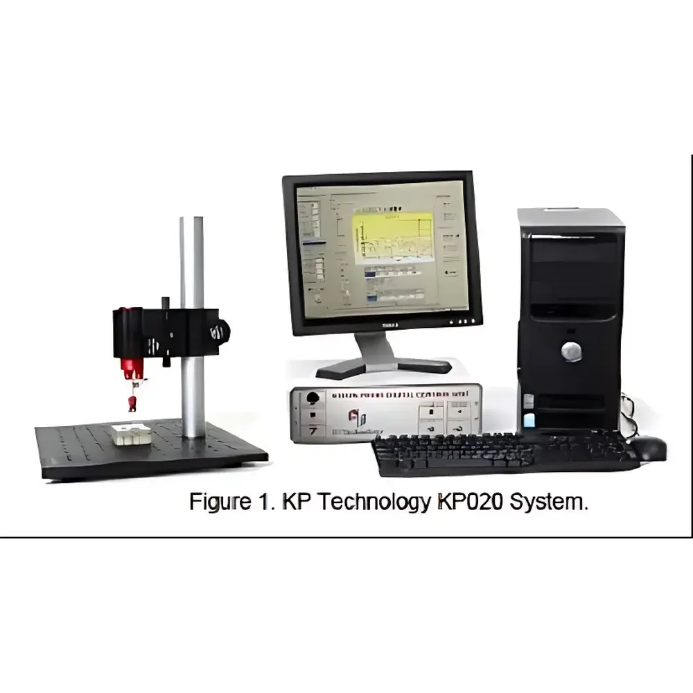
KP Technology KP010 Single-Point Kelvin Probe System
| Origin | UK |
|---|---|
| Manufacturer Type | Distributor |
| Origin Category | Imported |
| Model | KP010 |
| Pricing | Upon Request |
Overview
The KP Technology KP010 Single-Point Kelvin Probe System is a precision electrostatic measurement instrument engineered for non-contact, non-destructive characterization of surface potential and work function on conductive, semiconducting, and insulating materials. Based on the vibrating capacitor (Kelvin probe force microscopy) principle, the system measures the contact potential difference (CPD) between a vibrating metallic reference probe and the sample surface without physical contact or charge injection. This enables quantitative determination of local electronic surface properties—specifically, the work function, which is governed by the topmost 1–3 atomic or molecular layers. As such, the KP010 serves as a surface-sensitive analytical tool with applications spanning thin-film electronics, photovoltaic material screening, corrosion science, catalysis research, and dielectric interface studies. Its operation is grounded in classical electrostatic theory: when the probe vibrates at a fixed frequency near the sample, the resulting AC current is nulled by applying a DC bias—the null voltage directly corresponds to the CPD, from which work function is derived relative to the probe’s calibrated reference.
Key Features
- Industry-leading work function resolution of 1–3 meV (with 2 mm probe) and 5–10 meV (with 50 µm probe on optical vibration-isolation table)
- Voice-coil actuation—replacing piezoelectric drivers—to minimize mechanical drive noise and enhance long-term signal stability
- Zero-crossing detection circuitry that actively suppresses parasitic capacitance effects and improves signal-to-noise ratio beyond conventional lock-in amplification approaches
- Digital control architecture governing all probe parameters including vibration amplitude, frequency, phase, and feedback gain
- Integrated height regulation mechanism enabling precise, repeatable probe–sample gap control during both static measurement and lateral scanning
- Automatic distance tracking system maintaining constant probe–sample separation under thermal drift or mechanical perturbation
- Two interchangeable probe options: standard 2 mm diameter probe and high-spatial-resolution 50 µm probe
- Manual Z-axis translation stage (25.4 mm travel) with micrometer-driven fine positioning for coarse alignment and calibration
Sample Compatibility & Compliance
The KP010 accommodates planar solid samples up to 100 mm in diameter and 25 mm in thickness, including metals, doped and intrinsic semiconductors (e.g., Si, GaAs, perovskites), oxides (e.g., TiO₂, ITO), polymers, and passivated dielectrics. No conductive coating or vacuum environment is required; measurements are performed under ambient laboratory conditions (controlled humidity and temperature recommended). The system complies with fundamental metrological requirements for surface potential traceability and supports GLP-aligned documentation workflows. While not certified to ISO/IEC 17025, its digital control architecture and audit-ready parameter logging facilitate integration into regulated environments requiring documented measurement uncertainty and instrument qualification per ASTM E2778 (Standard Guide for Surface Potential Measurements Using Kelvin Probe Force Microscopy).
Software & Data Management
The proprietary KPSuite software provides full digital control of all hardware parameters via USB 2.0 interface. It features intuitive GUI-based setup for vibration tuning, feedback loop optimization, and CPD nulling. A guided signal optimization wizard simplifies initial alignment and maximizes SNR without requiring advanced electronics expertise. Real-time measurement mode captures up to 1,000 data points per minute at ~20 meV resolution—ideal for monitoring dynamic work function shifts during gas exposure, illumination, or thermal cycling. All raw and processed data are saved in HDF5 format with embedded metadata (timestamp, probe ID, environmental conditions, operator ID), ensuring FAIR (Findable, Accessible, Interoperable, Reusable) data principles. Export options include CSV, MATLAB (.mat), and ASCII for third-party analysis. Audit trail functionality records parameter changes, user logins, and measurement sessions—supporting 21 CFR Part 11 readiness when paired with institutional identity management.
Applications
- Quantitative work function mapping of transparent conductive oxides (TCOs) for OLED and OPV device optimization
- In situ monitoring of surface dipole formation during self-assembled monolayer (SAM) deposition
- Corrosion onset detection via localized work function gradients on coated metals
- Photogenerated surface photovoltage (SPV) analysis using optional SPV020 module under monochromatic illumination
- Interface band alignment determination at heterojunctions (e.g., organic/inorganic, 2D/3D) through CPD profiling
- Charge trapping dynamics in gate dielectrics and ferroelectric films
- Environmental aging studies of polymer–metal interfaces under controlled humidity and UV exposure
FAQ
What vacuum level is required for KP010 operation?
None—the system operates under ambient atmospheric conditions. Optional glovebox integration is available for inert-atmosphere or low-humidity measurements.
Can the KP010 be used for lateral scanning?
Yes—the base configuration supports manual point-by-point mapping; it is field-upgradeable to motorized XY scanning (KP-SCAN option) with sub-micron positional repeatability.
Is calibration traceable to national standards?
The probe work function is calibrated against polycrystalline gold (Φ = 5.1 eV ± 0.02 eV, NIST-traceable reference) using in-situ CPD referencing protocols.
How does the voice-coil driver improve measurement stability?
It eliminates piezoelectric hysteresis and thermal drift while providing linear, broadband mechanical response—critical for maintaining consistent vibration amplitude and phase over multi-hour acquisitions.
What sample preparation is required?
Minimal: samples must be flat, clean, and electrically isolated. No sputtering, etching, or vacuum-compatible mounting is needed. Standard SEM stubs or custom holders with spring-loaded electrical contact are compatible.