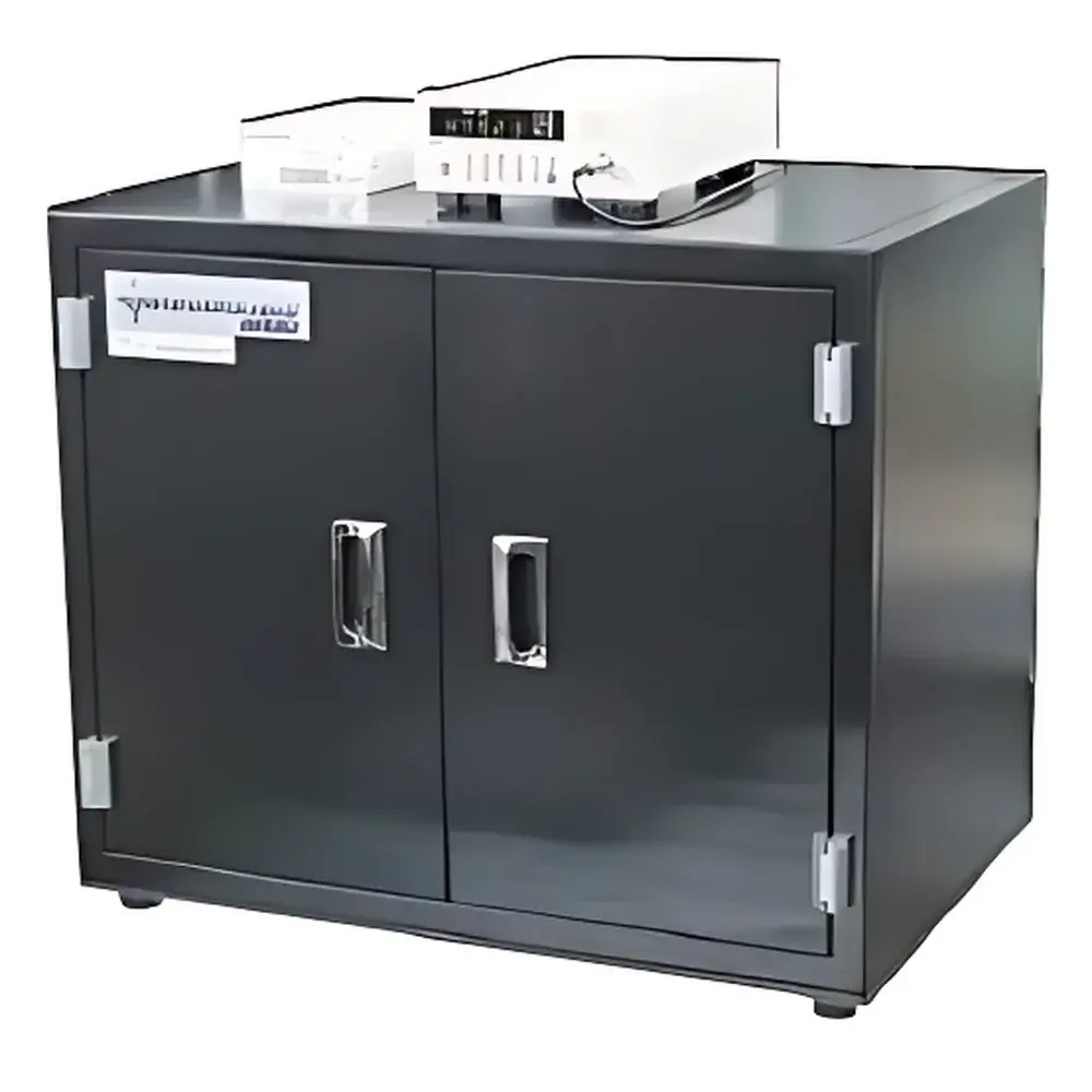
LBIC Laser-Induced Current Mapping System LBC-2
| Origin | Japan |
|---|---|
| Manufacturer Type | Authorized Distributor |
| Origin Category | Imported |
| Model | LBC-2 |
| Price Range | USD 70,000 – 112,000 |
| Instrument Type | Benchtop |
| Integration | Fully Integrated System |
Overview
The LBIC Laser-Induced Current Mapping System LBC-2 is a precision benchtop instrument engineered for spatially resolved photocurrent characterization of optoelectronic devices. It operates on the principle of laser-induced current (LBIC) mapping—a non-contact, localized excitation technique where a focused monochromatic laser beam scans across a device under test (DUT) while measuring the resulting short-circuit current (Isc) at each position. This method enables quantitative assessment of lateral photoresponse uniformity, carrier collection efficiency, and interfacial defects without electrical contact to active layers—critical for R&D and quality assurance in emerging photovoltaic technologies. Designed specifically for thin-film and solution-processed devices, the LBC-2 delivers 10 µm spatial resolution over a 50 × 50 mm measurement area, making it especially suited for evaluating perovskite solar cells fabricated by spin-coating, where edge-to-center compositional and crystallinity gradients commonly induce performance non-uniformity.
Key Features
- Fully integrated benchtop architecture with embedded electrometer, XY translation stage, laser source, sample chamber, and dedicated control PC—no external cabling or alignment required.
- Standard 532 nm continuous-wave green laser (Class 2, ≤1 mW output, ±5% stability/hour) with optional wavelength expansion via SMA-coupled diode lasers (375–904 nm), enabling spectral responsivity analysis and quantum efficiency (QE) derivation.
- High-precision motorized XY stage with ±25 mm travel range and 0.01 mm minimum step resolution, synchronized with real-time current acquisition.
- Ultra-low-noise current measurement capability spanning 10 fA to 20 mA, supporting both high-sensitivity perovskite film evaluation and robust SiPD/CCD/CMOS sensor characterization.
- Integrated manual shutter and software-controlled automatic shutter mechanism for precise irradiation timing and dark-current baseline subtraction.
- Onboard visible-light camera system for real-time laser spot monitoring and sample positioning verification within the enclosed chamber (W750 × D270 × H650 mm).
Sample Compatibility & Compliance
The LBC-2 accommodates rigid and flexible substrates up to 50 × 50 mm, including glass, ITO/PET, silicon wafers, and encapsulated perovskite devices. Its open-electrode configuration supports four-terminal sensing when combined with external bias sources (optional). The system complies with IEC 60825-1:2014 for Class 2 laser safety and meets electromagnetic compatibility requirements per EN 61326-1. Data acquisition and reporting workflows support GLP/GMP-aligned documentation practices, with timestamped metadata, user audit trails, and exportable raw datasets compatible with ISO/IEC 17025 traceability frameworks.
Software & Data Management
Controlled via Windows 7 (32-bit) native software, the LBC-2 platform provides intuitive scan setup, real-time current visualization, and post-processing tools for quantitative uniformity analysis. Software calculates spatial metrics including local current density, normalized deviation [(Imax − Imin) / (Imax + Imin) × 100%], mean effective current, and standard deviation across user-defined regions. Export formats include CSV, ASCII, and native binary files; 3D surface plots and false-color current maps are generated directly. All measurement parameters—including laser wavelength, power, dwell time, stage coordinates, and electrometer settings—are embedded in file headers for full experimental reproducibility. The software architecture supports integration with laboratory information management systems (LIMS) via standardized APIs.
Applications
- Perovskite solar cell optimization: identification of coating non-uniformity, pinhole distribution, and interfacial recombination zones.
- Thin-film photodetector (SiPD, InGaAs PD) homogeneity validation prior to wafer-level testing.
- CMOS and CCD sensor pixel response mapping for defect localization and QE calibration.
- Transparent conductive oxide (TCO) and charge transport layer (e.g., NiOx, SnO2) screening in multilayer device stacks.
- Accelerated degradation studies under localized laser stress with concurrent current monitoring.
FAQ
What laser wavelengths are supported natively, and how is wavelength switching implemented?
The system ships with a fixed 532 nm laser module. Optional wavelengths (375, 406, 445, 473, 488, 635, 650, 670, 785, 808, 830, 850, 904, and 980 nm) are delivered as plug-and-play SMA-coupled diode modules requiring no optical realignment.
Is the system compatible with external biasing or environmental control?
Yes—dedicated BNC ports allow integration with programmable voltage sources for biased LBIC (BLBIC) measurements. Sample chamber access ports support optional temperature stages or inert-gas purging kits (not included).
How is current calibration performed, and what uncertainty level is achievable?
Calibration uses NIST-traceable reference resistors and shunt standards; typical measurement uncertainty is ±0.8% of reading (k = 2) for currents >100 pA, per internal validation reports.
Can the software generate reports compliant with ISO 17025 or FDA 21 CFR Part 11?
While the base software does not include electronic signatures or audit trail encryption, raw data and metadata exports fully support downstream integration into validated LIMS or ELN platforms meeting those regulatory requirements.