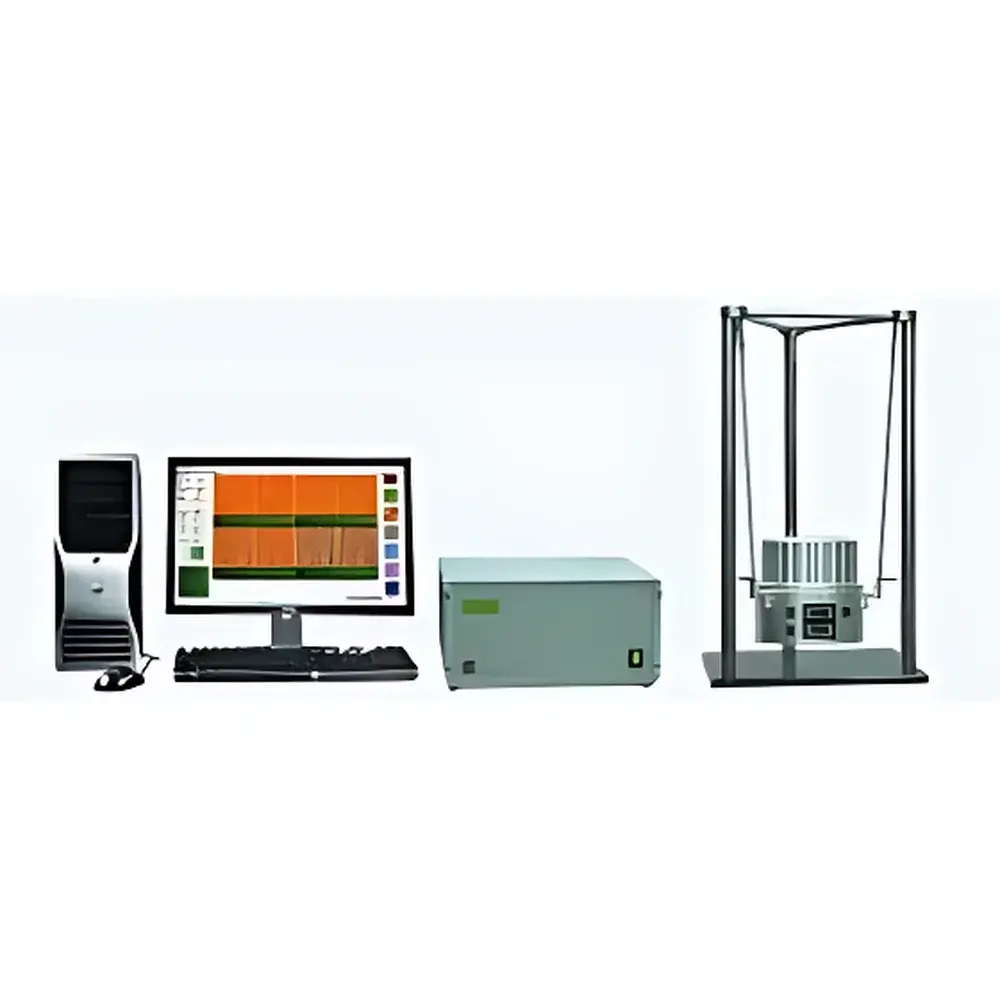
BENYUAN Nano CSPM5500 Scanning Probe Microscope (SPM) — Integrated AFM/STM/LFM Platform
| Brand | BENYUAN Nano |
|---|---|
| Model | CSPM5500 |
| Origin | Beijing, China |
| Instrument Type | Atomic Force Microscope (AFM) with integrated Scanning Tunneling Microscope (STM) and Lateral Force Microscope (LFM) |
| Position Detection Noise | 0.1 nm |
| Sample Diameter Limit | <102 mm (4 in) |
| Sample Thickness Limit | <40 mm |
| XY Sample Stage Travel Range | 100 mm × 100 mm |
| Maximum Z-Travel (Auto-Approach) | >30 mm |
| Image Resolution | Up to 4096 × 4096 physical pixels |
| Horizontal Resolution (AFM) | 0.2 nm (mica-calibrated) |
| Vertical Resolution (AFM) | 0.1 nm (mica-calibrated) |
| Horizontal Resolution (STM) | 0.1 nm (graphite-calibrated) |
| Vertical Resolution (STM) | 0.01 nm (graphite-calibrated) |
| Data Interface | Fast Ethernet (10/100 Mbps) or USB 2.0 |
| Real-Time 3D Visualization | Yes |
| PID-Controlled Force Feedback | Yes |
Overview
The BENYUAN Nano CSPM5500 is a research-grade, multi-modal scanning probe microscope engineered for high-fidelity nanoscale characterization in academic, industrial, and metrology laboratories. Launched in August 2008, it integrates three core SPM techniques—Atomic Force Microscopy (AFM), Scanning Tunneling Microscopy (STM), and Lateral Force Microscopy (LFM)—within a single, thermally stable mechanical architecture. Its operational principle relies on piezoelectric actuation for sub-nanometer tip positioning, combined with optical beam deflection (for AFM) and quantum tunneling current detection (for STM) to resolve surface topography, electronic structure, and nanomechanical properties at atomic and near-atomic resolution. Designed for reproducible quantitative analysis, the CSPM5500 complies with fundamental metrological traceability requirements: all spatial calibrations are validated using NanoSensors-certified reference samples, traceable to the Physikalisch-Technische Bundesanstalt (PTB), Germany’s national metrology institute. This ensures data integrity across inter-laboratory comparisons and supports compliance with ISO/IEC 17025–aligned quality management systems.
Key Features
- Multi-mode imaging platform supporting contact, tapping, phase imaging (AFM), constant-current and constant-height (STM), and friction loop/load/constant-load mapping (LFM)
- Sub-angstrom vertical resolution in STM mode (0.01 nm, graphite-calibrated) and 0.1 nm vertical noise floor in AFM mode
- Automated, one-click sample approach with >30 mm Z-travel—enabling rapid engagement of large or uneven specimens without manual pre-alignment
- Dual-stage precision sample positioning: coarse (motorized 100 mm × 100 mm XY stage) and fine (micrometer-adjustable tilt/rotation) for accurate region-of-interest targeting
- High-resolution acquisition up to 4096 × 4096 physical pixels per scan, preserving true nanoscale fidelity even over micrometer-scale fields
- Advanced real-time PID feedback control for force regulation—optimized for stable imaging at elevated scan speeds (up to 10× faster than conventional analog-loop systems)
- Front-panel 16×4 LCD display providing immediate status feedback on laser alignment, cantilever resonance, feedback gain, and scanner voltage
- Native support for real-time 3D surface rendering during acquisition—facilitating dynamic interpretation of evolving topographic features
Sample Compatibility & Compliance
The CSPM5500 accommodates standard wafer formats (≤4-inch diameter) and thick substrates (≤40 mm), making it suitable for semiconductor wafers, thin-film electrodes, biomaterials on mica/glass, and bulk conductive or insulating samples. Its modular design permits optional integration of environmental enclosures (controlled humidity/temperature), liquid cells, and conductive or magnetic probes—enabling operation under ambient, vacuum, or liquid-phase conditions. Calibration protocols follow ISO 25178-601 (areal surface texture) and ASTM E2450 (AFM calibration standards). While not certified for GMP manufacturing environments, its audit-ready data logging, timestamped parameter tracking, and non-modifiable raw data export (in proprietary .spm and open .txt formats) align with GLP documentation practices and support FDA 21 CFR Part 11–compatible electronic record workflows when paired with validated third-party LIMS or ELN software.
Software & Data Management
The system ships with BENYUAN’s proprietary SPMControl v5.x suite, offering intuitive instrument control, real-time image processing (FFT filtering, plane leveling, cross-section extraction), and comprehensive curve analysis (force-distance, amplitude-distance, I-V, I-Z). All acquired images and spectroscopic data are stored with embedded metadata—including date/time stamp, user ID, scanner calibration coefficients, and environmental conditions—ensuring full experimental provenance. Raw datasets export in ASCII-compatible formats for interoperability with MATLAB, Gwyddion, SPIP, and commercial statistical analysis tools. The software supports batch processing, scripting via Python API (via optional SDK), and direct integration into networked lab infrastructures via TCP/IP or shared folder protocols.
Applications
The CSPM5500 serves as a foundational tool for materials science, nanoelectronics, surface physics, and soft matter research. Typical use cases include: atomic-resolution lattice imaging of 2D materials (graphene, MoS₂); nanomechanical property mapping (elastic modulus, adhesion) of polymer blends and composites; nanoscale friction and wear analysis of lubricated interfaces; in situ electrochemical AFM of battery electrode degradation; and nanolithography via dip-pen nanolithography (DPN) or local oxidation. Its STM capability enables band structure probing of topological insulators and quantum dot arrays, while LFM provides quantitative tribological insights relevant to MEMS/NEMS device reliability assessment.
FAQ
Is the CSPM5500 compatible with ultra-high vacuum (UHV) environments?
No—the base configuration is designed for ambient and controlled-atmosphere operation. UHV compatibility requires custom chamber integration and is not supported out-of-the-box.
Can the system perform electrical property mapping beyond basic STM?
Yes—optional modules include Conductive AFM (CAFM), Kelvin Probe Force Microscopy (KPFM), and Scanning Capacitance Microscopy (SCM), enabling work function, surface potential, and carrier concentration profiling.
What level of technical support and calibration services does BENYUAN Nano provide internationally?
BENYUAN Nano offers remote diagnostics, application consulting, and annual recalibration services through authorized regional partners. PTB-traceable calibration certificates are issued upon request for metrology-critical deployments.
Does the software support automated image stitching across multiple scan fields?
Yes—SPMControl v5.x includes mosaic stitching with sub-pixel registration accuracy, enabling seamless large-area topographic reconstruction up to 1 mm × 1 mm.
Are third-party probes fully compatible with the CSPM5500?
The system accepts standard 12.7 mm × 12.7 mm AFM/STM probe holders and supports most commercial cantilevers (e.g., Bruker, Nanoworld, BudgetSensors), including conductive, magnetic, and high-speed variants—with automatic resonance frequency detection and Q-factor compensation.