Benyuan Nano BY3000 Atomic Force Microscope
| Brand | Benyuan Nano |
|---|---|
| Origin | Beijing, China |
| Manufacturer Type | Authorized Distributor |
| Country of Origin | China |
| Model | BY3000 |
| Price Range | USD 14,000 – 72,000 |
| Instrument Type | Atomic Force Microscope (AFM) |
| Position Detection Noise | 0.1 nm |
| Maximum Sample Diameter | 45 mm |
| Maximum Sample Thickness | 15 mm |
| XY Sample Stage Travel Range | 100 mm × 100 mm |
Overview
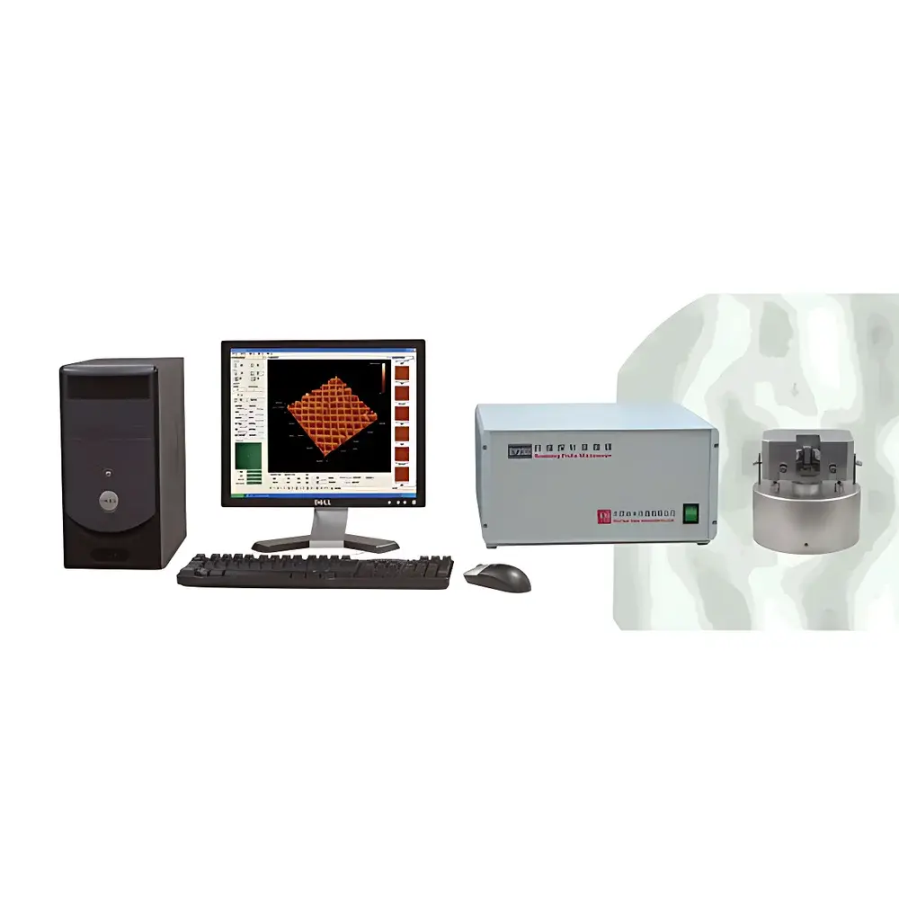
The Benyuan Nano BY3000 Atomic Force Microscope is a high-stability, multi-mode scanning probe microscope engineered for nanoscale surface characterization in academic research laboratories and industrial quality control environments. Based on the principle of mechanical probe–surface interaction detection via laser beam deflection on a micro-cantilever, the BY3000 delivers true atomic-resolution topographic imaging under ambient conditions. Its modular architecture supports interchangeable operational modes—including contact-mode AFM, tapping-mode AFM, lateral force microscopy (LFM), scanning tunneling microscopy (STM), and force–distance spectroscopy—enabling comprehensive nanomechanical, electrical, and tribological property mapping. The system integrates a TI 32-bit digital signal processor (DSP) core with real-time operating system firmware, ensuring deterministic control timing and sub-millisecond response latency critical for dynamic mode stability and quantitative force calibration.
Key Features
- Sub-nanometer positioning noise floor (≤0.1 nm RMS) achieved through low-drift piezoelectric scanners and optimized optical lever detection
- Large-sample chamber design accommodating specimens up to 45 mm in diameter and 15 mm in thickness—ideal for wafers, coatings, biological substrates, and composite materials
- Motorized 100 mm × 100 mm XY sample stage with programmable navigation, enabling automated multi-region survey scans and large-area stitching
- Five-channel high-voltage amplifier module (APEX integrated) for precise Z-axis actuation and fast-response feedback control
- Fully automated tip approach sequence eliminating manual coarse positioning; intelligent probe recognition ensures correct parameter initialization per cantilever type
- Dual-mode compatibility: seamless switching between AFM and STM configurations via standardized probe holder interchange—no hardware reconfiguration required
- Fast Ethernet (10/100 Mbps) interface for deterministic data streaming, remote operation, and integration into centralized lab networks
Sample Compatibility & Compliance
The BY3000 accommodates a broad range of conductive and non-conductive samples—including semiconductor wafers, polymer films, thin-film solar cells, biomaterials (e.g., collagen fibrils, cell membranes), and ceramic coatings—without requiring conductive coating for most AFM modalities. Its open-stage architecture allows custom environmental accessories (e.g., liquid cells, temperature-controlled stages) to be integrated externally. While not certified to ISO/IEC 17025 or FDA 21 CFR Part 11 out-of-the-box, the system’s full raw data export capability (including time-stamped force curves, photodiode voltage traces, and DAC/ADC logs) supports traceable analysis workflows compliant with GLP and GMP documentation standards. All image metadata—including scan parameters, calibration constants, and instrument state flags—are embedded in saved files for audit-ready reporting.
Software & Data Management
The BY3000 operates under a native Windows-based software suite supporting Windows XP through Windows 10 (32- and 64-bit). It provides synchronized acquisition across up to five analog input channels during a single scan, permitting concurrent topography, phase, friction, current, and Z-sensor signals. Real-time 3D rendering enables immediate visual validation of surface features, while batch processing tools automate roughness analysis (Ra, Rq, Rz, Rsk, Rku) and particle statistics per ISO 25178 and ASTM E2942. Image reconstruction algorithms include tip convolution modeling and deconvolution-based sharpening. All datasets are saved in vendor-neutral binary formats (.dat, .txt) with ASCII headers, ensuring long-term archival integrity and third-party compatibility with MATLAB, Python (NumPy), and Gwyddion.
Applications
- Nanomaterial morphology and dispersion analysis (e.g., graphene oxide flakes, quantum dots, metal–organic frameworks)
- Thin-film uniformity and interfacial defect inspection in photovoltaic and display manufacturing
- Mechanical property mapping via nanoindentation and force spectroscopy (elastic modulus, adhesion energy, deformation hysteresis)
- Biological soft matter characterization—cell stiffness, membrane elasticity, protein aggregation kinetics—in air or liquid environments
- Failure analysis of microelectromechanical systems (MEMS), including stiction assessment and surface wear profiling
- Quantitative roughness certification for optical components, medical implants, and precision machined surfaces per ISO 4287/4288
FAQ
Does the BY3000 support vacuum or low-temperature operation?
The standard configuration operates under ambient atmospheric conditions. Vacuum and cryogenic compatibility require optional external enclosures and are not included in the base system.
What probe types are compatible with the BY3000?
Standard silicon and silicon nitride cantilevers with nominal spring constants from 0.01 N/m to 40 N/m are supported. STM probes must meet <100 Ω tip resistance and <5 µm apex radius specifications.
Is the software compliant with FDA 21 CFR Part 11 requirements?
The software includes user authentication, electronic signature prompts, and audit trail logging. Full Part 11 compliance requires site-specific validation documentation and network-level access controls implemented by the end user.
Can the system perform automated grain size or particle analysis?
Yes—the built-in analysis module calculates particle count, area-equivalent diameter, aspect ratio, and convex hull metrics directly from height images, with output conforming to ISO 13322-2 guidelines.
What is the maximum achievable scan speed at full resolution?
At 512 × 512 pixels and 1 Hz line rate, the system achieves stable imaging with ≤5% distortion; maximum usable frame rate depends on feedback bandwidth settings and sample topography complexity, typically ranging from 0.1 to 5 Hz for high-fidelity data acquisition.