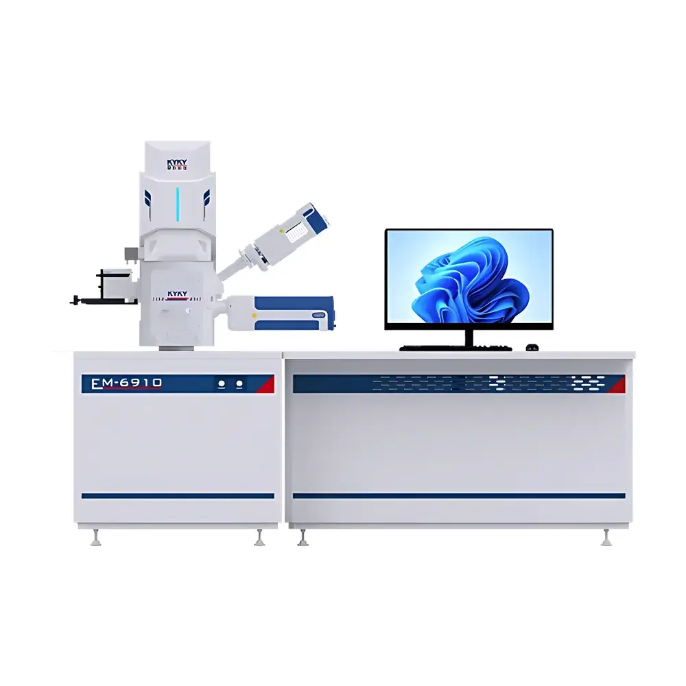
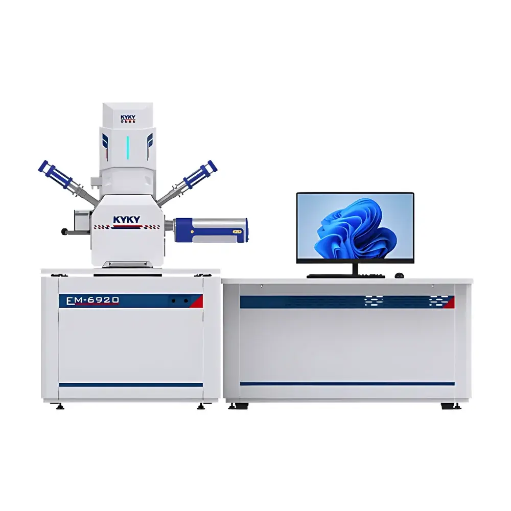
KYKY-EM69 Series Tungsten-Filament Scanning Electron Microscope
| Brand | KYKY |
|---|---|
| Origin | Beijing, China |
| Manufacturer Type | Direct Manufacturer |
| Instrument Class | Floor-Standing Conventional SEM |
| Electron Source | Tungsten Filament |
| SEM Category | Entry-Level Tungsten-Filament SEM |
| Secondary Electron (SE) Resolution | 3 nm @ 30 kV, 8 nm @ 3 kV |
| Accelerating Voltage Range | 0.2–30 kV |
| Backscattered Electron (BSE) Resolution | 4 nm @ 30 kV |
| Sample Chamber | Optional Large-Capacity Chamber |
| Vacuum Mode | Compatible with Low-Vacuum Module |
| Load Lock System | Max. Sample Diameter ≤75 mm, Height ≤15 mm |
| Navigation Camera | Integrated Wide-Field CCD Navigation Camera |
| Imaging Modes | Simultaneous SE/BSE Dual-Channel Imaging |
| Image Stitching | Automated Full-Field Matrix Acquisition & Real-Time High-Throughput Mosaic Reconstruction |
| Particle Analysis | AI-Driven Morphometric Quantification (size, aspect ratio, circularity, convexity, Feret diameter, etc.) with Auto-Scale Calibration |
| Metrology Tools | Distance, Angle, Line (horizontal/vertical), Circle Diameter, and Profile Analysis |
| Electron Beam Lithography (EBL) Capability | Integrated Vector-Scan EBL Subsystem Supporting Pattern Definition, Dose Control, and Concurrent SEM Observation |
Overview
The KYKY-EM69 Series is a floor-standing, tungsten-filament scanning electron microscope engineered for robust performance in academic laboratories, industrial quality control environments, and applied research facilities requiring reliable high-resolution surface imaging without the operational complexity or cost of field-emission systems. Based on conventional thermionic emission principles, the EM69 utilizes a stable, long-life tungsten hairpin filament operating under high-vacuum conditions (with optional low-vacuum compatibility via dedicated gas injection module), delivering consistent beam current and reproducible imaging across a wide accelerating voltage range (0.2–30 kV). Its optical architecture integrates electromagnetic condenser and objective lens systems optimized for depth of field and signal-to-noise ratio at both high-kV (material contrast, BSE composition mapping) and low-kV (surface topography, charge-sensitive specimens) regimes. Designed for routine operation by technicians and researchers alike, the system emphasizes mechanical stability, thermal drift mitigation, and intuitive workflow integration—making it particularly suitable for materials characterization, failure analysis, geological sample screening, and life science specimen evaluation where quantitative morphology and compositional contrast are essential.
Key Features
- Integrated load-lock chamber enabling rapid sample exchange (<2 minutes) without breaking main column vacuum—critical for high-throughput labs and multi-user facilities.
- Modular vacuum architecture supporting optional low-vacuum mode (up to 130 Pa) for imaging non-conductive or hydrated specimens without metal coating.
- Dual-channel simultaneous acquisition of secondary electron (SE) and backscattered electron (BSE) signals, allowing real-time correlation between topographic and atomic-number-dependent contrast.
- Wide-field navigation camera with motorized stage coordination for precise region-of-interest targeting and macro-to-micro transition.
- Automated large-area image stitching using adaptive field matrix planning and GPU-accelerated alignment algorithms—capable of reconstructing gigapixel-scale mosaics from hundreds of individual frames with sub-pixel registration accuracy.
- Embedded electron beam lithography (EBL) subsystem with vector-scan pattern generator, enabling nanoscale maskless patterning while retaining full SEM imaging functionality on the same platform.
Sample Compatibility & Compliance
The EM69 accommodates standard 32 mm pin-mount stubs and optional extended-height holders (up to 15 mm height, 75 mm diameter). Its modular chamber design supports custom stage configurations—including tilt/rotate, heating, cooling, and tensile stages—subject to mechanical and vacuum interface specifications. The system meets ISO 14644-1 Class 5 cleanroom handling recommendations for column assembly and conforms to IEC 61000-6-3 (EMC emission) and IEC 61000-6-2 (immunity) standards. All software operations—including image acquisition, annotation, measurement logging, and EBL recipe storage—support audit-trail generation compliant with GLP documentation requirements. While not certified to FDA 21 CFR Part 11 out-of-the-box, the system’s user authentication, electronic signature, and immutable data export protocols enable validation pathways for regulated environments.
Software & Data Management
The proprietary KYKY-SEM Suite provides a unified interface for instrument control, image processing, metrology, and analytical quantification. It features a hierarchical project-based file structure with embedded metadata (kV, WD, dwell time, detector gain, stage coordinates, timestamp). Particle analysis employs convolutional neural networks trained on synthetic and empirical SEM datasets to segment particles independent of threshold artifacts, automatically calibrating scale bars using fiducial markers or stage encoder feedback. Measurement results—including Feret diameter distributions, convex hull area ratios, and angular orientation histograms—are exportable to CSV, Excel, or HDF5 formats. All raw images are stored in lossless TIFF format with 16-bit depth; stitched mosaics support pyramidal tiling for web-based viewing via compatible DICOM or OME-TIFF viewers.
Applications
- Materials Science: Fractography of metals and composites; grain boundary analysis in sintered ceramics; inclusion identification in steel alloys; cross-sectional interface inspection in thin-film stacks.
- Geosciences: Mineral phase discrimination via BSE Z-contrast; pore network quantification in shale and reservoir rocks; microfossil morphology reconstruction.
- Electronics & Nanotechnology: Defect review on PCB substrates; solder joint integrity assessment; nanoparticle dispersion uniformity in conductive inks; EBL-defined quantum dot arrays.
- Life Sciences: Freeze-fracture replication of cell membranes; pollen grain morphotyping; biofilm architecture mapping on medical device surfaces.
- Industrial QA/QC: Coating thickness estimation via edge profiling; wear debris classification in lubricants; fiber diameter distribution in nonwovens.
FAQ
What vacuum levels does the EM69 support in low-vacuum mode?
The optional low-vacuum module maintains pressures between 10–130 Pa, enabling direct imaging of insulating or beam-sensitive samples without sputter coating.
Can the EBL subsystem be used concurrently with live SEM imaging?
Yes—the vector-scan EBL engine operates independently of the primary imaging scan generator, allowing real-time observation of exposure progress and immediate post-exposure verification without stage repositioning.
Is third-party software integration supported for particle analysis?
Raw TIFF exports include calibrated pixel dimensions and metadata tags compatible with open-source platforms such as ImageJ/Fiji, Python (scikit-image, OpenCV), and commercial packages including MATLAB and Thermo Scientific Avizo.
Does the system support automated stage calibration for repeatable coordinate referencing?
Stage calibration routines—using grid-patterned reference samples and encoder-based homing—enable sub-micron positional repeatability across multiple sessions, facilitating correlative microscopy workflows.
What maintenance intervals are recommended for the tungsten filament?
Typical filament lifetime exceeds 150 operating hours under standard 20–30 kV conditions; replacement is performed via front-access cartridge design and requires no column venting.


