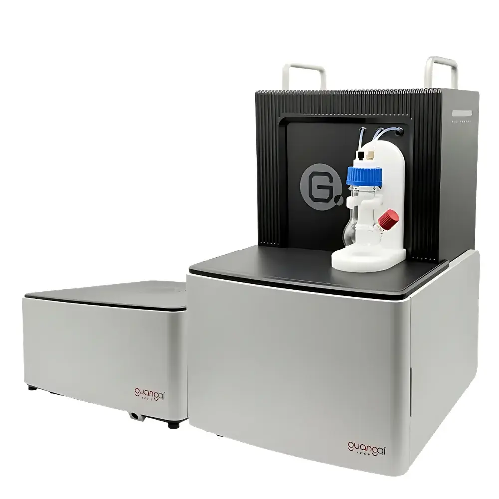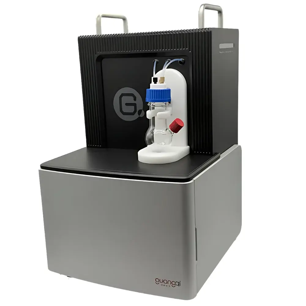
LatticeAx 225 Wafer Dicing Saw
| Origin | USA |
|---|---|
| Manufacturer Type | Authorized Distributor |
| Origin Category | Imported |
| Model | LatticeAx 225 |
| Price Range | USD $14,000 – $43,000 (FOB) |
| Maximum Blade Feed Rate | 500–600 mm/min |
| Application Scope | R&D Laboratories & Pilot-Scale Packaging Lines |
Overview
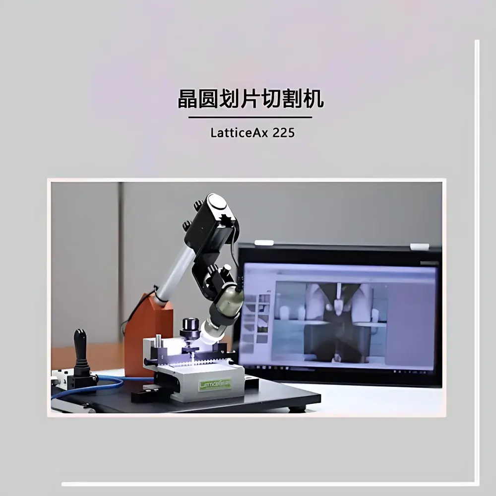
The LatticeAx 225 Wafer Dicing Saw is a precision micro-dicing instrument engineered for semiconductor research, MEMS development, and advanced packaging prototyping. It employs mechanical blade-based dicing with controlled scribe-and-break methodology—optimized for low-stress, high-fidelity separation of brittle substrates including silicon, SiC, GaN, quartz, glass, and ceramic wafers. Unlike high-speed rotary saws designed for high-volume production, the LatticeAx 225 prioritizes positional accuracy, repeatability, and surface integrity in non-production laboratory environments. Its core architecture integrates a rigid granite base, kinematically stabilized stage, and real-time optical feedback loop to enable sub-20 µm placement accuracy—critical for small-die, heterogeneous integration, and failure analysis workflows where conventional alignment tolerances are insufficient.
Key Features
- Sub-20 µm positioning accuracy achieved via integrated high-magnification digital microscopy with polarized illumination and motorized fine-focus control
- Dedicated industrial-grade platform with vibration-damped granite base and air-isolated motion stages for stable indentation and cutting under load
- USB 2.0 digital microscope interface with real-time image acquisition, on-screen crosshair overlay, and coordinate referencing for target-specific scribe placement
- Pneumatically actuated vacuum chuck with programmable pressure control for secure fixation of wafers ranging from 50 mm to 200 mm in diameter and thicknesses from 100 µm to 1.5 mm
- Modular blade handling system compatible with standard diamond-coated dicing blades (e.g., #1000–#4000 grit), supporting both full-cut and partial-depth scribe modes
- No consumable calibration routines or scheduled maintenance intervals—designed for continuous operation in ISO Class 5–7 cleanroom-adjacent lab settings
Sample Compatibility & Compliance
The LatticeAx 225 accommodates diverse substrate geometries and material systems commonly encountered in semiconductor R&D: single-crystal silicon (100/111), SOI, compound semiconductors (GaAs, InP), wide-bandgap materials (SiC, AlN), fused silica, borosilicate glass, LTCC/HTCC ceramics, and thin-film metalized wafers. Sample mounting requires no adhesive tape or UV-curable films—relying instead on vacuum-only fixation to preserve post-dice surface quality and eliminate residue-related contamination risks. The system complies with SEMI S2-0201 safety guidelines and meets CE electromagnetic compatibility (EMC) requirements. While not certified for GMP manufacturing, its traceable motion control, repeatable parameter logging, and audit-ready operation logs support GLP-aligned documentation per ISO/IEC 17025 laboratory accreditation frameworks.
Software & Data Management
Operation is managed through a Windows-based native application supporting intuitive point-and-click workflow sequencing. All critical parameters—including scribe coordinates (X/Y/Z), blade depth, feed rate, vacuum pressure, and imaging exposure time—are digitally recorded per run and exported in CSV or XML format. The software includes built-in pass/fail criteria evaluation against user-defined tolerance bands (e.g., ±20 µm positional deviation), generating summary reports suitable for internal QA review or external audit submission. Data files retain embedded timestamps, operator ID, and system firmware version—enabling full traceability aligned with FDA 21 CFR Part 11 principles when deployed in regulated development labs.
Applications
- Low-volume die singulation for reliability testing (HAST, TCT, HTSL) and electrical characterization
- Preparation of test structures for TEM cross-sectioning and FIB-SEM site-specific milling
- Prototyping of chiplet-based assemblies requiring precise edge geometry and minimal chipping
- Back-end-of-line (BEOL) process validation for redistribution layer (RDL) and fan-out wafer-level packaging (FOWLP)
- Failure analysis sample preparation where mechanical cleavage must avoid thermal damage or delamination
- Academic and government lab use in nanoelectronics, photonic IC, and quantum device fabrication
FAQ
What wafer thicknesses can the LatticeAx 225 accommodate?
Standard configuration supports wafers from 100 µm to 1.5 mm thick. Optional stage adapters extend compatibility to ultra-thin (<50 µm) handled wafers using carrier bonding protocols.
Is the system compatible with automated wafer handling or cluster tools?
No—it is a standalone benchtop instrument intended for manual loading and operator-guided operation. Integration with robotic handlers requires third-party OEM interface development.
Does the microscope support measurement annotation and scale calibration?
Yes. The imaging software includes pixel-to-micron calibration using NIST-traceable stage movement, plus on-screen distance, angle, and area measurement tools with exportable overlays.
Can the system perform stealth dicing or laser-assisted scribing?
No. The LatticeAx 225 is exclusively a mechanical dicing platform. It does not incorporate laser, plasma, or waterjet modules.
What maintenance is required beyond routine cleaning?
None. The system contains no oil-lubricated mechanisms, belt drives, or consumable wear parts. Daily wipe-down of the vacuum chuck and weekly inspection of blade-mounting torque are the only recommended procedures.