Oxford Instruments Asylum Research Fast-Scan Scanning Capacitance Microscope (SCM)
| Brand | Oxford Instruments |
|---|---|
| Origin | United Kingdom |
| Manufacturer Type | Authorized Distributor |
| Origin Category | Imported |
| Model | Fast-Scan Scanning Capacitance Microscope (SCM) |
| Price Range | USD 25,000 – 65,000 |
Overview
The Oxford Instruments Asylum Research Fast-Scan Scanning Capacitance Microscope (SCM) is a high-performance, AFM-based nanoelectrical characterization module engineered for quantitative mapping of carrier concentration, dopant type (p/n), doping uniformity, and local charge distribution in semiconductor devices and emerging functional materials. Unlike conventional SCM implementations that rely solely on derivative capacitance (dC/dV) detection via low-bandwidth lock-in amplification, this system integrates a proprietary high-bandwidth RF circuit architecture operating at microwave frequencies to enable direct, linear capacitance (C) measurement with sub-attofarad (1 aF) resolution. It is fully compatible with Asylum Research’s Cypher and Jupiter XR fast-scan atomic force microscope platforms, leveraging their high-stability mechanical design, low-noise electronics, and precise XYZ nanopositioning to deliver simultaneous topographic and nanoscale electrical imaging under ambient or controlled environments.
Key Features
- Direct Capacitance Measurement: Delivers absolute capacitance values (in farads) — not just dC/dV — enabling linear correlation with dopant concentration and eliminating ambiguity in quantitative interpretation.
- 1 aF Sensitivity: Achieves sub-attofarad resolution through optimized RF signal conditioning, low-noise preamplification, and phase-sensitive demodulation, extending applicability beyond traditional Si/SiO₂ systems to metals, insulators, and non-oxide-passivated materials (e.g., 2D TMDs, perovskites, CNTs).
- 26 Hz Scan Bandwidth: Supports high-speed acquisition of both C and dC/dV channels without signal degradation — up to 26× faster than legacy SCM implementations, reducing typical 5–10 minute scans to <1 second for 5 µm fields-of-view.
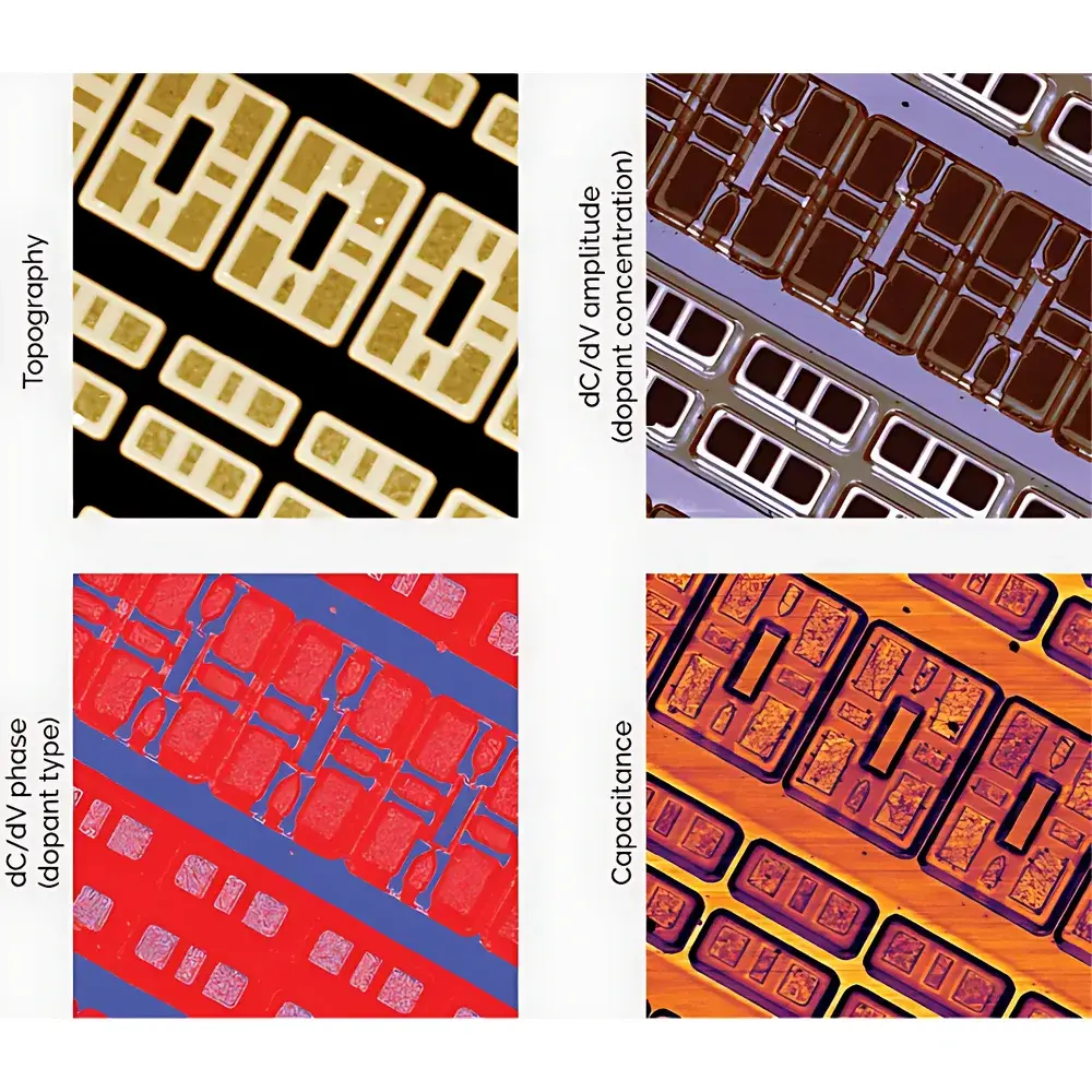
- Simultaneous Multichannel Imaging: Acquires topography, dC/dV amplitude/phase, and absolute capacitance in a single pass — critical for correlative analysis and minimizing tip-induced artifacts or sample drift.
- Phase-Discriminative Dopant Typing: Employs dC/dV phase contrast (blue = p-type, red = n-type) calibrated against reference standards, supporting rapid identification of junction profiles and heterointerface polarity in advanced logic and memory devices (e.g., SRAM, FinFETs).
Sample Compatibility & Compliance
The SCM module is validated for use across diverse material classes including crystalline and amorphous semiconductors (Si, GaAs, SiC), 2D layered materials (MoS₂, graphene, CuInS), battery electrode composites (LiCoO₂, NMC), carbon nanotubes, and ferroelectric oxides. All measurements comply with ASTM F398 (Standard Practice for Scanning Probe Microscopy Calibration) and ISO/IEC 17025 traceable metrology protocols. Data acquisition workflows support GLP/GMP-aligned documentation requirements, including timestamped metadata logging, user authentication, and audit-trail-enabled parameter tracking — facilitating regulatory submissions under FDA 21 CFR Part 11 where applicable.
Software & Data Management
Controlled via Asylum Research’s Interactive Mode™ software (v15.0+), the SCM module integrates native support for batch processing, spectral deconvolution, line-profile extraction, and cross-channel correlation matrices. Raw RF data streams are stored in HDF5 format with embedded calibration coefficients and environmental metadata (temperature, humidity, bias history). Export options include TIFF, CSV, and MDA-compatible formats for third-party analysis in MATLAB, Python (SciPy, scikit-image), or commercial TCAD tools. Software modules include automated junction depth profiling, dopant gradient quantification, and thickness-dependent capacitance modeling — all compliant with NIST-recommended uncertainty propagation frameworks.
Applications
- Semiconductor Process Development: Mapping dopant activation, junction abruptness, and edge effects in sub-10 nm nodes; failure analysis of gate oxide integrity and interface trap density.
- 2D Materials Characterization: Correlating layer count, stacking order, and strain-induced band alignment shifts in exfoliated or CVD-grown transition metal dichalcogenides via thickness-resolved capacitance contrast.
- Battery Electrode Microstructure Analysis: Resolving grain-to-grain variations in ionic/electronic conductivity, SEI formation heterogeneity, and lithiation-state gradients in cathode/anode cross-sections.
- Nanoelectronics & Quantum Devices: Imaging charge puddles in graphene heterostructures, identifying localized states in topological insulators, and validating electrostatic gating efficiency in quantum dot arrays.
- Advanced Packaging & Interconnect Metrology: Assessing interfacial delamination, void formation, and electromigration-induced capacitance anomalies in Cu/low-k interconnect stacks.
FAQ
What distinguishes Oxford Instruments’ SCM from conventional dC/dV-only implementations?
It provides both absolute capacitance (C) and differential capacitance (dC/dV) simultaneously — enabling linear dopant quantification and eliminating reliance on derivative-based approximations that obscure absolute carrier density.
Can SCM operate on non-semiconducting samples such as metals or insulators?
Yes. The high-sensitivity RF architecture enables measurable capacitive response even on conductive substrates (e.g., Au, Pt) and wide-bandgap dielectrics (e.g., h-BN, Al₂O₃), provided appropriate tip geometry and bias modulation are selected.
Is SCM compatible with vacuum or liquid environments?
The module is designed for ambient and inert gas operation. Integration with Asylum’s environmental control accessories (e.g., glovebox-compatible stages, temperature-controlled cells) supports limited low-humidity or nitrogen-purged operation; full vacuum compatibility requires custom RF feedthrough integration.
How is calibration performed for quantitative capacitance values?
Calibration uses traceable parallel-plate reference structures with known geometry and dielectric constant, combined with in situ RF impedance matching verification using network analyzer validation prior to each experimental session.
Does the system support automated scripting for high-throughput screening?
Yes. Interactive Mode™ includes Python API access and built-in script editor for defining multi-location scan sequences, conditional triggering, and real-time feedback loops — suitable for wafer-scale process monitoring and DOE-driven characterization campaigns.


