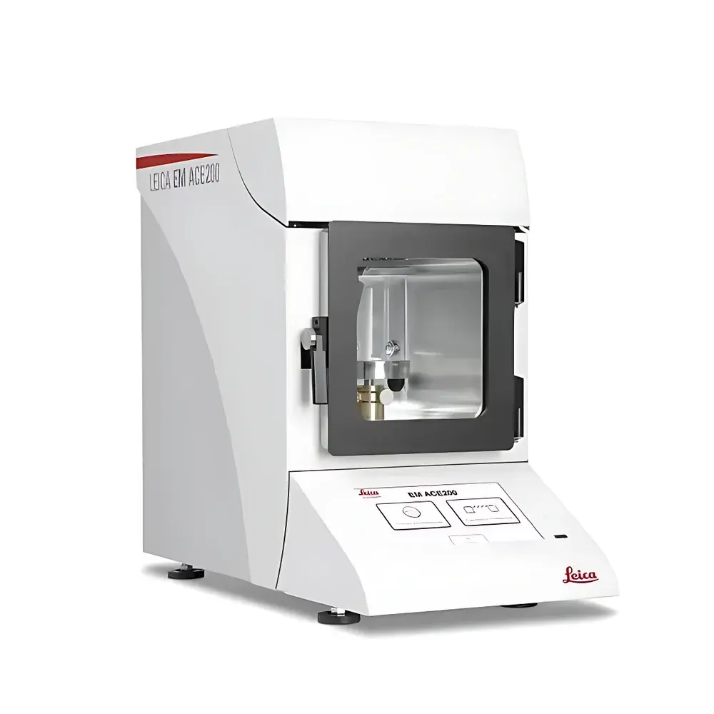
Leica EM ACE200 Low-Vacuum Coating System
| Brand | Leica |
|---|---|
| Origin | Germany |
| Model | EM ACE200 |
| Coating Modes | Sputter Coating (Au, Pt, Pd, Cr, etc.) & Carbon Evaporation (Carbon Filament) |
| Vacuum Range | 1 × 10⁻¹ to 5 × 10⁻¹ mbar |
| Chamber Diameter | 140 mm |
| Chamber Height | 120 mm |
| Sample Stage | Motorized Planetary Rotation (Optional) |
| Thickness Monitoring | Quartz Crystal Microbalance (QCM) Optional |
| Glow Discharge | Optional Integrated Module |
| Compliance | CE, RoHS, ISO 9001 Certified |
| Software Control | EM ACE200 Touch Interface with Predefined & Custom Protocols |
Overview
The Leica EM ACE200 is a benchtop low-vacuum coating system engineered for high-reproducibility conductive and ultra-thin coatings in electron microscopy sample preparation. Operating in the 1 × 10⁻¹–5 × 10⁻¹ mbar pressure range, it supports two primary physical vapor deposition (PVD) techniques: magnetron sputtering for metallic films (e.g., Au, Pt, Pd, Cr, Ir) and resistive carbon evaporation using high-purity carbon filaments. Unlike high-vacuum thermal evaporators, the ACE200’s optimized low-pressure environment enables rapid pump-down (<60 s to operational vacuum), reduced contamination risk, and stable plasma generation for uniform sputter deposition—critical for preserving fine surface topography in SEM and TEM specimens. Its modular architecture allows seamless switching between sputter and carbon heads without tooling or realignment, ensuring consistent geometry and film stoichiometry across coating modalities.
Key Features
- Modular dual-mode design: Interchangeable sputter and carbon evaporation heads mounted on a shared vacuum chamber platform, enabling method-specific optimization without cross-contamination.
- Motorized planetary rotation stage (optional): Ensures uniform coating thickness distribution across irregular or multi-sample substrates, validated per ASTM E1558 for coating homogeneity assessment.
- Integrated quartz crystal microbalance (QCM) option: Provides real-time thickness monitoring with ±0.1 nm resolution for carbon layers and ±0.2 nm for metal films, traceable to NIST-traceable calibration standards.
- Glow discharge module (optional): Enables hydrophilic surface activation of TEM grids and polymer substrates prior to carbon coating, improving film adhesion and reducing charging artifacts.
- Touchscreen-driven automation: Preloaded protocols for common applications (e.g., “SEM-Au Sputter”, “TEM-Carbon Grid”) with adjustable parameters (current, time, pressure, rotation speed); all settings stored with timestamped audit trails compliant with GLP documentation requirements.
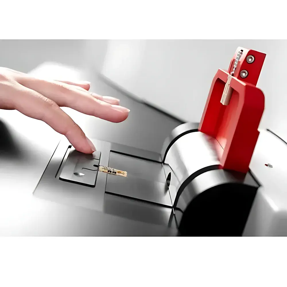
- Service-friendly engineering: Front-accessible chamber with quick-release door, removable internal shielding, tool-free filament replacement, and LED-lit interior for visual inspection—designed for routine maintenance by lab personnel without field engineer support.
Sample Compatibility & Compliance
The EM ACE200 accommodates standard SEM stubs (up to 50 mm diameter), TEM grids (200–400 mesh), silicon wafers (up to 4″), and custom holders for fragile or non-planar specimens (e.g., pollen, diatoms, fractured ceramics). All vacuum components comply with ISO 8573-1 Class 4 compressed air purity standards when interfaced with external gas lines. The system meets CE marking requirements under the EU Machinery Directive 2006/42/EC and Electromagnetic Compatibility Directive 2014/30/EU. Optional QCM and glow discharge modules are validated per ISO/IEC 17025:2017 for metrological traceability in accredited laboratories. Full electronic logs—including vacuum curves, power delivery profiles, and user authentication IDs—are exportable as CSV or PDF for FDA 21 CFR Part 11-compliant data archiving.
Software & Data Management
Control is executed via an embedded Linux-based touchscreen interface (7″ capacitive display) with intuitive icon-driven navigation. Protocol libraries include >25 factory-validated methods spanning life science (e.g., cryo-SEM gold/palladium sputtering), materials science (Cr/Pt bilayer for EBSD), and nanotechnology (ultra-thin carbon for graphene transfer). Each run generates a structured metadata file containing operator ID, date/time stamp, chamber pressure history, current/voltage waveforms, and final QCM reading. Data export supports USB storage or network transfer (SFTP/SCP) to LIMS or ELN systems. Audit trail functionality records all parameter modifications, user logins, and emergency stop events with SHA-256 hashing for integrity verification.
Applications
- SEM sample preparation: High-conductivity Au/Pd coatings (2–10 nm) for charge dissipation on insulating biological tissues, polymers, and geological sections.
- TEM grid coating: Electron-transparent amorphous carbon films (3–8 nm) for supporting beam-sensitive specimens; optional Cr underlayer for enhanced mechanical stability.
- EBSD analysis: Ultra-smooth Cr or Ni coatings (≤5 nm) minimizing diffraction pattern distortion during orientation mapping.
- ToF-SIMS and XPS: Ultra-clean carbon films deposited under glow-discharged conditions to minimize hydrocarbon background interference.
- Microfabrication: Maskless metallization of MEMS devices using shadow-mask-compatible stage positioning.
FAQ
What vacuum level is required for stable sputtering with the EM ACE200?
Stable DC magnetron sputtering is achieved at 2–3 × 10⁻¹ mbar using argon process gas; no turbomolecular pump is required—the integrated dual-stage rotary vane pump suffices.
Can the system deposit alloys or multi-layer stacks?
Yes—sequential deposition is supported via programmable head-swapping and vacuum-hold protocols; alloy sputtering (e.g., Au-Pd) requires co-sputtering from dual targets (not included as standard).
Is remote monitoring or integration with laboratory automation systems possible?
The system supports Modbus TCP and RS-232 interfaces for integration with central lab management software; OEM SDK available for custom API development.
How often does the carbon filament require replacement?
Typical lifetime exceeds 150 coating cycles at 10 nm thickness; filament wear is monitored via real-time resistance tracking and logged in the system diagnostics report.
Does Leica provide IQ/OQ documentation for regulated environments?
Yes—factory-verified Installation Qualification (IQ) and Operational Qualification (OQ) packages are available upon request, aligned with ISO/IEC 17025 and GMP Annex 15 guidelines.