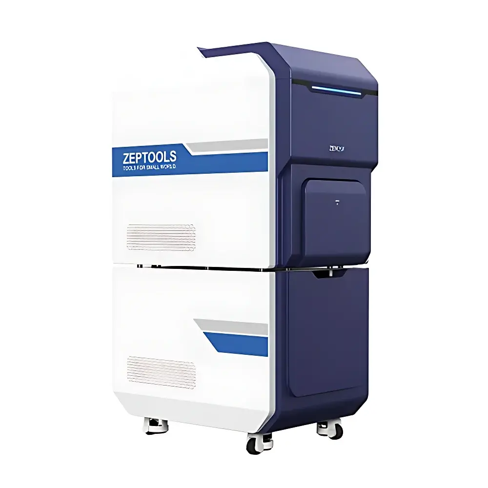
ZEPTOOLS ZEM Ultra Desktop Field Emission Scanning Electron Microscope
| Brand | ZEPTOOLS |
|---|---|
| Origin | Anhui, China |
| Model | ZEM Ultra |
| Instrument Type | Desktop SEM |
| Electron Source | Schottky Field Emission Gun |
| SEM Class | High-Resolution Field Emission SEM |
| Maximum Magnification | 1,000,000× |
| Accelerating Voltage | 1–15 kV (continuously adjustable) |
| Backscattered Electron (BSE) Resolution | ≤2.5 nm |
| Maximum Sample Dimensions | 176 mm (W) × 185 mm (L) × 125 mm (H) |
| Stage Options | XY, XYZ, XYT, or 5-Axis Motorized Stage |
| Standard Detectors | BSE, SE, EDS |
| Vacuum Architecture | Triple-Independent Vacuum System |
| Imaging Modes | SE, BSE, Deceleration Mode (optional, 0–10 kV sample bias) |
| Navigation | Integrated Chamber Camera + Optical Navigation System |
| Image Formats | 512×512 (real-time video), 2048×2048 (high-res acquisition) |
| Automation | Auto Focus, Auto Brightness/Contrast, Large-Area Stitching |
| In Situ Capability | Compatible with in situ stages (heating, cooling, tensile, electrical biasing) |
| Detector Expansion | EBSD, CL, STEM-in-SEM |
Overview
The ZEPTOOLS ZEM Ultra Desktop Field Emission Scanning Electron Microscope is an engineered solution for high-resolution microstructural characterization in academic laboratories, quality control facilities, and industrial R&D environments where space, operational simplicity, and analytical versatility are critical constraints. Unlike conventional floor-standing SEMs, the ZEM Ultra integrates a thermally assisted Schottky field emission electron source into a compact, self-shielded desktop platform—delivering sub-3 nm resolution without requiring dedicated high-voltage rooms or cryogenic infrastructure. Its measurement principle relies on raster-scanning a focused electron beam across conductive or coated specimens while collecting secondary electrons (SE), backscattered electrons (BSE), and characteristic X-rays via energy-dispersive spectroscopy (EDS). The triple-independent vacuum architecture ensures rapid pump-down times (8 h drift <1.5 nm at 100,000×), and robust immunity to hydrocarbon contamination—key performance attributes for routine daily use in non-dedicated microscopy labs.
Key Features
- Schottky field emission gun delivering high brightness (>10⁸ A/cm²·sr) and exceptional long-term stability—enabling consistent imaging at 1–15 kV accelerating voltage with minimal beam-induced damage to beam-sensitive materials.
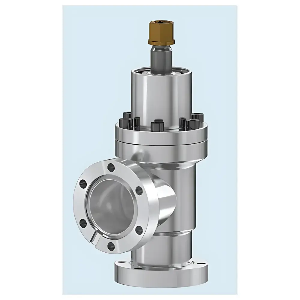
- Triple-stage independent vacuum system (ion pump + turbomolecular pump + getter pump) maintaining base pressure <2×10⁻⁷ Pa in the gun chamber and <5×10⁻⁵ Pa in the specimen chamber—critical for preserving emitter lifetime and minimizing surface contamination during EDS mapping.
- Modular motorized stage options (XY, XYZ, XYT, or full 5-axis) with ±1° tilt and 360° rotation capability—supporting comprehensive angular analysis, cross-sectional imaging, and multi-angle EBSD pattern acquisition.
- Integrated optical navigation system with 10× magnification chamber camera—enabling precise region-of-interest selection prior to electron beam engagement, reducing setup time by up to 60% compared to manual alignment workflows.
- Real-time auto-focus and auto-brightness/contrast algorithms compliant with ISO 16700:2016 guidelines for automated SEM operation—ensuring reproducible image optimization across operators and shifts.
- Native support for large-area stitching (up to 10,000×10,000 pixels) with sub-pixel registration accuracy—facilitating quantitative grain size distribution analysis and defect mapping over millimeter-scale regions.
Sample Compatibility & Compliance
The ZEM Ultra accommodates specimens up to 176 mm wide × 185 mm long × 125 mm tall, making it compatible with standard silicon wafers (up to 200 mm), battery electrode cross-sections, composite laminates, and geological thin sections. Conductive coating (Au/Pd or C) is optional for non-conductive samples; low-voltage imaging (≤3 kV) combined with deceleration mode (0–10 kV sample bias) enables charge-free observation of polymers, ceramics, and biological tissues. All vacuum, electrical safety, and electromagnetic compatibility designs conform to IEC 61000-6-3 (EMI) and IEC 61010-1 (safety). The instrument’s software architecture supports audit trails, user role management, and electronic signatures per FDA 21 CFR Part 11 requirements when configured with optional GLP/GMP compliance modules.
Software & Data Management
Acquisition and analysis are managed through ZEPTOOLS’ proprietary SEM Suite v4.x—a Windows-based application built on Qt and HDF5 data architecture. It provides real-time EDS spectrum acquisition with live elemental overlay, line-scan quantification (ZAF correction), and phase identification via library matching (Oxford Instruments AZtec-compatible format). All raw images, spectra, and metadata are stored in vendor-neutral HDF5 files with embedded EXIF-like tags (accelerating voltage, working distance, dwell time, detector gain). Data export supports TIFF (16-bit), CSV (spectral data), and MSA (EDS) formats. Remote access, batch processing scripts (Python API), and integration with LIMS via RESTful endpoints are available under enterprise licensing.
Applications
- Materials science: Grain boundary analysis in Ni-based superalloys, porosity quantification in additively manufactured Ti-6Al-4V, and intermetallic phase identification in aluminum matrix composites.
- Electronics: Failure analysis of solder joints, delamination detection in PCB stacks, and nanoscale defect inspection in GaN HEMT devices.
- Life sciences: Morphological assessment of freeze-fractured cell membranes, collagen fiber orientation in decellularized scaffolds, and mineralization gradients in bone biopsies.
- Geosciences: Clay mineral classification via BSE contrast and EDS compositional zoning in zircon crystals.
- Quality assurance: Coating thickness verification on automotive catalyst substrates, particle size distribution in pharmaceutical inhaler powders, and fiber diameter uniformity in nonwoven filtration media.
FAQ
Is the ZEM Ultra suitable for uncoated biological samples?
Yes—when operated at ≤3 kV with deceleration mode enabled and using low-noise in-lens SE detection, the system achieves sufficient surface sensitivity and charge dissipation for hydrated or lightly fixed tissues without metal sputtering.
Can EBSD be added post-purchase?
Yes—the column port is pre-aligned and mechanically compatible with industry-standard EBSD detectors (e.g., Oxford Symmetry, EDAX Velocity). Installation requires only software license activation and calibration routines.
What vacuum maintenance is required?
No consumable vacuum components require periodic replacement; the ion pump and getter elements are rated for >15,000 hours of continuous operation. Annual preventive maintenance includes turbomolecular pump oil inspection and chamber cleaning per ISO 14644-1 Class 5 cleanroom protocols.
Does the system support automated particle analysis?
Yes—via optional ParticleMetric module, which performs ISO 13322-1 compliant size/shape classification on binary masks derived from SE/BSE thresholding, with statistical reporting per ASTM E1245-22.
Is remote training and service supported?
All software interfaces include built-in screen-sharing and remote diagnostic capabilities compliant with ISO/IEC 27001 information security standards; service engineers can initiate secure sessions with customer authorization.