Auniontech SPS Square-Pulsed Source Thermal Property Measurement System
| Brand | Auniontech |
|---|---|
| Origin | Shanghai, China |
| Manufacturer Type | Authorized Distributor |
| Product Category | Domestic |
| Model | SPS |
| Pricing | Upon Request |
Overview
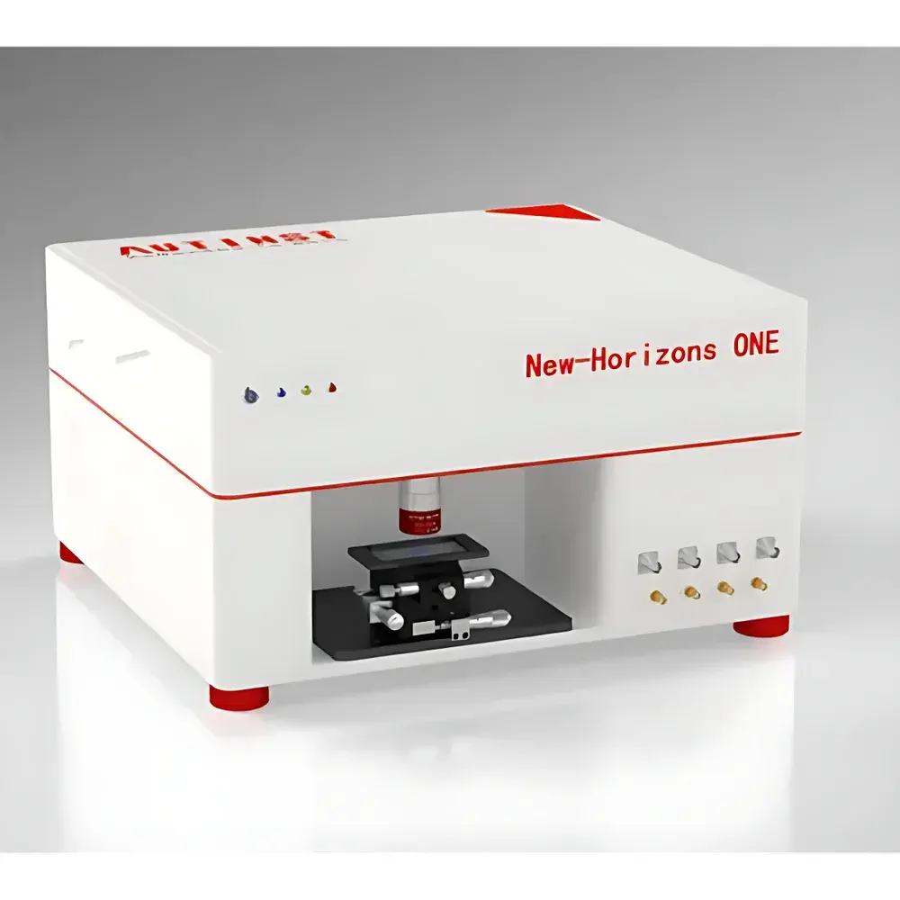
The Auniontech SPS Square-Pulsed Source Thermal Property Measurement System is a high-precision, laser-based time-domain thermoreflectance platform engineered for comprehensive thermal characterization of microscale and sub-millimeter samples. Unlike conventional steady-state or transient methods constrained by macroscopic assumptions, the SPS system implements the Square-Pulsed Source (SPS) methodology—a rigorously validated extension of pump-probe thermoreflectance—enabling simultaneous, model-based extraction of thermal conductivity (k), volumetric heat capacity (ρcp), and interfacial thermal resistance (Rth) from a single experimental dataset. The technique operates on the physical principle that a square-wave modulated pump laser induces periodic temperature oscillations in a nanoscale metal transducer layer (typically ~100 nm Au or Al), while a collinear or off-axis probe beam monitors reflectivity changes linearly proportional to surface temperature rise (ΔT < 10 K). By acquiring amplitude and phase responses across a broad modulation frequency range (1 Hz – 20 MHz), the system reconstructs thermal transport behavior governed by Fourier’s law and the heat diffusion equation, with full support for isotropic, orthotropic, and fully anisotropic thermal conductivity tensor reconstruction in three dimensions.
Key Features
- Multi-modal operation: Unified platform supporting SPS (square-pulsed source), SDTR (spatial-domain thermoreflectance), and SSTR (steady-state thermoreflectance) measurement protocols within a single optical configuration
- Dual-wavelength pump-probe architecture: 458 nm pump laser (200 mW max output, 50% duty cycle square modulation) and 785 nm probe laser optimized for signal-to-noise ratio and minimal thermal penetration depth
- Adjustable optical resolution: Variable spot radius from 1 µm to 40 µm via motorized beam shaping optics, enabling spatially resolved thermal mapping and localized interface analysis
- Integrated CCD microscopy: Real-time visual alignment and sample surface inspection with 10×–50× magnification and sub-micron registration accuracy
- Fully automated workflow: Motorized stage control, auto-focus, laser power calibration, and closed-loop feedback during data acquisition reduce operator dependency and improve inter-lab reproducibility
- Advanced signal processing: Periodic waveform analysis (PWA) engine performs real-time lock-in detection, multi-harmonic fitting, and simultaneous parameter inversion for k, ρcp, Rth, and anisotropy ratios—with built-in uncertainty propagation based on measurement noise statistics and model sensitivity matrices
Sample Compatibility & Compliance
The SPS system accommodates freestanding thin films (≥20 nm), epitaxial heterostructures (e.g., Si/SiO2, GaN/AlN, MoS2/h-BN), bulk single crystals, polycrystalline ceramics, and composite laminates. Sample mounting is compatible with standard TEM grids, silicon wafers (up to 200 mm), and custom substrates with conductive or insulating backing. All measurement routines adhere to ASTM E1461 (Standard Test Method for Thermal Diffusivity of Solids by the Flash Method) and ISO 22007-2 (Plastics — Determination of Thermal Conductivity and Thermal Diffusivity — Part 2: Transient Plane Source Method) foundational principles, while data traceability supports GLP-compliant reporting requirements. Raw waveform data, fitted parameters, covariance matrices, and residual plots are stored in HDF5 format with embedded metadata compliant with FAIR (Findable, Accessible, Interoperable, Reusable) data principles.
Software & Data Management
The proprietary SPS Control Suite v4.x provides a unified GUI for instrument orchestration, experiment design, and post-processing. It includes preconfigured templates for common material classes (metals, dielectrics, semiconductors, 2D materials), customizable heating protocols (single-frequency sweep, multi-tone excitation, chirped modulation), and export modules for MATLAB, Python (NumPy/Pandas), and CSV. Audit trails record all user actions, hardware states, environmental conditions (ambient temperature, humidity), and software versioning per measurement session. For regulated environments, optional 21 CFR Part 11 compliance package adds electronic signatures, role-based access control, and immutable raw-data archiving with SHA-256 checksum validation.
Applications
- Thermal management R&D for advanced packaging: Quantifying through-silicon via (TSV) thermal resistance and Cu/low-k interface conductance in 3D IC stacks
- Characterization of thermoelectric thin films: Decoupling cross-plane k and ρcp to calculate figure-of-merit (ZT) without destructive cross-sectioning
- Anisotropic phonon transport in layered materials: Resolving in-plane vs. cross-plane thermal conductivity tensors in transition metal dichalcogenides (TMDs) and van der Waals heterostructures
- Process development feedback for ALD/CVD: In-line monitoring of thermal property evolution during atomic-layer deposition of high-κ gate dielectrics
- Validation of ab initio lattice dynamics simulations: Experimental benchmarking of predicted phonon dispersion and mean free path distributions
FAQ
What sample preparation is required for SPS measurements?
A continuous, optically reflective metal transducer layer (~100 nm Au or Al) must be deposited uniformly on the sample surface via e-beam evaporation or sputtering. Substrate roughness should be < 5 nm RMS; no electrical contact or vacuum bonding is needed.
Can the SPS system measure thermal properties of transparent or highly reflective materials?
Yes—by optimizing transducer adhesion and selecting appropriate pump/probe wavelengths (e.g., 532 nm pump for SiC, 808 nm for GaAs), the system achieves reliable thermoreflectance contrast across dielectrics, semiconductors, and metals.
Is cryogenic or elevated temperature operation supported?
The base system operates from 20 °C to 80 °C using integrated Peltier stages; optional liquid-nitrogen-cooled cold-finger stages extend the range to 8 K, with in situ temperature calibration traceable to ITS-90.
How does SPS differ from time-domain thermoreflectance (TDTR)?
SPS uses square-wave modulation instead of sinusoidal or pulsed excitation, yielding higher harmonic content and improved sensitivity to low-frequency thermal diffusion processes—particularly advantageous for thick films (>1 µm) and low-conductivity materials (< 1 W/m·K).
Does the system provide uncertainty quantification for derived parameters?
Yes—each measurement report includes 95% confidence intervals computed via Monte Carlo sampling of input noise distributions and Jacobian-based error propagation through the inverse heat conduction model.


