Wave500 & Wave700 Wavelength Dispersive Spectrometer (WDS) by Oxford Instruments
| Brand | Oxford Instruments |
|---|---|
| Origin | United Kingdom |
| Model | Wave500, Wave700 |
| Detector Integration | Ultim Max EDS |
| Geometry | Focusing Rowland Circle with Curved Crystals |
| Energy Resolution | <10 eV at Mn Kα |
| Detection Limit | <100 ppm (typical, matrix-dependent) |
| Slit Mechanism | Motorized Incident Slit for Resolution/Background Optimization |
| Mounting Configuration | Tilted Geometry for Enhanced SEM Compatibility and Reproducible Sample Positioning |
| Compliance | Designed for integration with Zeiss SEM platforms (e.g., GeminiSEM, Sigma, Merlin) |
Overview
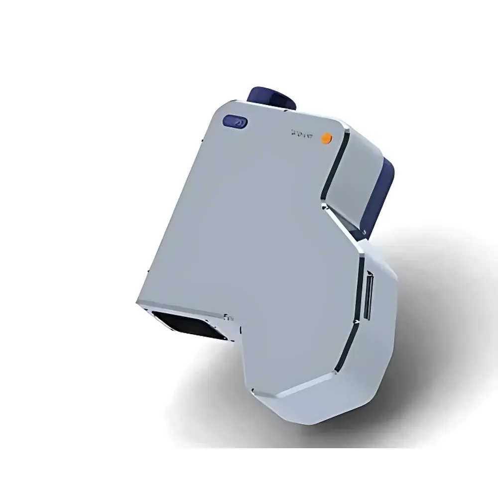
The Oxford Instruments Wave500 and Wave700 are high-performance wavelength dispersive spectrometers (WDS) engineered for quantitative elemental microanalysis in scanning electron microscopy (SEM) environments. Unlike energy-dispersive X-ray spectroscopy (EDS), WDS operates on Bragg diffraction principles: characteristic X-rays emitted from the sample strike curved, analytically optimized crystals mounted on a precise goniometer, where only wavelengths satisfying the Bragg condition (nλ = 2d sinθ) are focused onto a gas-flow proportional counter. This physical dispersion mechanism delivers intrinsic energy resolution typically below 10 eV at Mn Kα—over an order of magnitude better than conventional Si(Li) or SDD-based EDS detectors. As a result, the Wave series resolves overlapping peaks (e.g., S Kα/Pb Mα, Ti Kβ/V Kα, rare-earth L-lines) that remain inseparable in EDS spectra, enabling rigorous quantification of light elements (B–F), transition metals in complex alloys, and trace constituents (<100 ppm) in geological, metallurgical, and semiconductor specimens. The system is not a standalone instrument but a modular, vacuum-compatible WDS add-on designed for seamless integration with field-emission SEMs—particularly Zeiss Gemini-series platforms—where spatial resolution, beam stability, and stage repeatability are critical to analytical fidelity.
Key Features
- Focusing Rowland circle geometry with thermally stable, bent LiF, PET, TAP, and LDE crystals—enabling simultaneous multi-element coverage from B to U without mechanical reconfiguration
- Motorized incident slit assembly providing real-time optimization of spectral resolution versus peak-to-background ratio—critical for low-concentration analysis and overlapping line deconvolution
- Tilted optical path design minimizing shadowing effects and maximizing solid-angle collection efficiency while maintaining compatibility with standard SEM chamber dimensions and stage travel ranges
- Direct digital goniometer control synchronized with SEM stage coordinates, ensuring sub-micron positional reproducibility across mapping and point-analysis routines
- Native interoperability with Oxford Instruments’ AZtecWave software platform—unifying WDS and Ultim Max EDS data acquisition, background modeling, and matrix correction (ZAF/φ(ρz)) within a single workflow
- Vacuum-integrated detector housing rated to ≤1×10⁻⁵ mbar, compatible with high-vacuum and low-vacuum SEM modes when used with differential pumping interfaces
Sample Compatibility & Compliance
The Wave500 and Wave700 support conductive and non-conductive solid samples up to 100 mm in diameter and 50 mm in height, including polished metallographic mounts, thin-film cross-sections, mineral grains, and ceramic fracture surfaces. Sample charging is mitigated via low-kV beam conditions (5–15 kV), beam deceleration, and optional charge compensation (e.g., beam-induced current or low-energy electron flood). All hardware and firmware comply with CE marking requirements and electromagnetic compatibility (EMC) Directive 2014/30/EU. Data acquisition and processing workflows align with GLP and GMP documentation standards; AZtecWave supports audit-trail logging, user-access controls, and electronic signatures per FDA 21 CFR Part 11 when deployed in regulated QA/QC laboratories. Method validation adheres to ISO 16554 (electron probe microanalysis) and ASTM E1508 (quantitative WDS analysis).
Software & Data Management
AZtecWave serves as the unified analytical engine, combining WDS peak identification, intensity integration, continuum subtraction, and φ(ρz) matrix corrections with EDS-based phase classification and elemental mapping. It features automated crystal selection logic, dynamic background modeling using polynomial and Voigt-profile fitting, and iterative overlap correction for adjacent lines (e.g., Cr Kβ–Mn Kα). Raw spectral data are stored in vendor-neutral .aztd format, exportable to ASCII, CSV, or NIST DTSA-II compliant files. Batch processing supports method templating, inter-laboratory calibration transfer, and statistical process control (SPC) chart generation. Data integrity safeguards include timestamped acquisition logs, version-controlled calibration databases, and checksum-verified raw spectrum archives.
Applications
- High-accuracy quantification of minor and trace elements in Ni-based superalloys, TiAl intermetallics, and high-entropy alloys where EDS suffers from peak interference and poor detection limits
- Light-element analysis (C, N, O, F) in nitrided steels, oxynitride ceramics, and battery cathode materials using LDE and PC2 crystals under ultra-high vacuum conditions
- Geochemical fingerprinting of zircon, monazite, and apatite via U–Th–Pb dating protocols requiring sub-100 ppm precision on radiogenic isotopes
- Failure analysis of semiconductor interconnects and solder joints—resolving Cu L-lines from Sn M-lines and detecting Pb segregation at grain boundaries
- Regulatory compliance testing per RoHS, REACH, and ELV directives—validating restricted substance thresholds down to 50–100 ppm in homogeneous materials
FAQ
What SEM models are certified for Wave500/Wave700 integration?
Oxford Instruments provides factory-tested integration kits and alignment protocols for Zeiss GeminiSEM 300, Sigma 300, and Merlin Compact systems. Custom mounting solutions are available for Thermo Scientific Quanta and JEOL JSM-IT800 platforms upon engineering review.
Can Wave operate simultaneously with Ultim Max EDS?
Yes—AZtecWave enables true concurrent WDS/EDS acquisition: EDS provides rapid survey spectra and phase ID, while WDS performs targeted high-resolution quantification on selected points or regions, all within a synchronized coordinate framework.
Is cryogenic cooling required for the WDS detector?
No—the gas-flow proportional counter operates at ambient temperature; no liquid nitrogen or Peltier cooling is needed, reducing operational complexity and consumable dependency.
How is spectrometer calibration maintained over time?
Calibration is performed using certified reference materials (e.g., NIST SRM 2100, BAM Fe–Cr–Ni alloys); AZtecWave stores crystal d-spacings, detector gain offsets, and goniometer zero positions in encrypted, versioned calibration files with automatic drift compensation during long-duration analyses.
Are replacement crystals and slits user-serviceable?
Crystal exchange requires vacuum break and goniometer realignment by trained service engineers; however, motorized slit modules and detector windows are field-replaceable using Oxford-certified toolkits and guided AR-assisted procedures in AZtecWave.


")