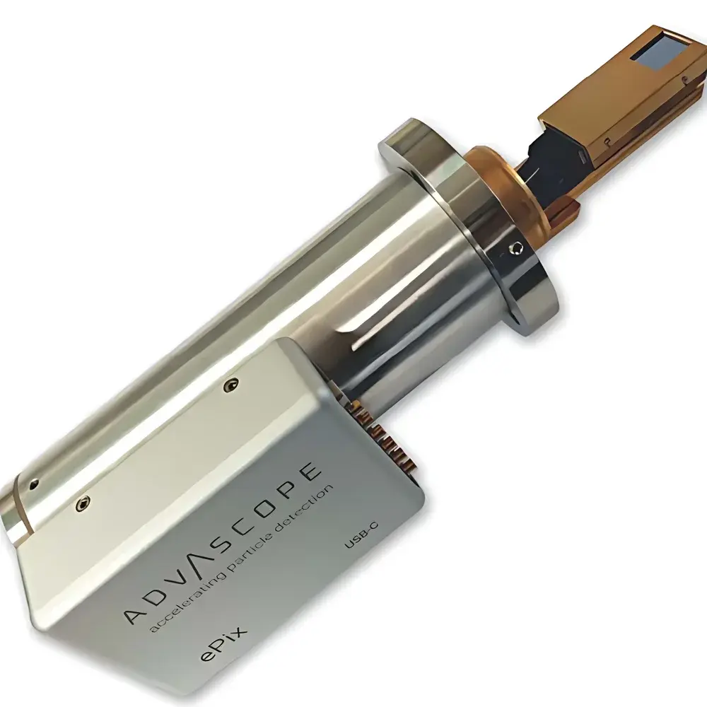
ePix® Timepix3 Direct Detection Electron Camera
| Brand | Advacam |
|---|---|
| Origin | Czech Republic |
| Model | ePix® |
| Sensor Technology | Timepix3-based hybrid pixel detector |
| Pixel Size | 55 × 55 µm |
| Pixel Matrix | 256 × 256 |
| Sensitive Area | 14 × 14 mm |
| Sensor Material | Silicon (Si), thickness options: 100, 300, 500 µm |
| Time-of-Arrival (TOA) Resolution | 1.56 ns |
| Maximum Hit Rate (Data-Driven Mode) | 64 Mhit/s |
| Energy Range | 2.5–300 keV |
| Readout Interface | USB-C |
| Power Consumption | 3.5 W |
| Operating Modes | Data-driven zero-suppressed, frame-based zero-suppressed |
| Pixel Operation Modes | Simultaneous Time-Over-Threshold (TOT) and Time-Of-Arrival (TOA), or integral TOT + event counting |
| Front-End Dimensions | 69 × 28 × 16 mm |
| Readout Unit Dimensions | 104 × 67 × 30 mm |
| Detector Mounting | Customizable mechanical interface |
| External Synchronization | LVDS I/O (Trigger In/Out, Clock In/Out, Ready In/Out) |
| Front-End to Readout Distance | Up to 45 cm |
| Thermal Management | Peltier-cooled, temperature-stabilized |
Overview
The ePix® Timepix3 Direct Detection Electron Camera is a high-performance hybrid pixel detector engineered for advanced electron microscopy applications requiring single-electron sensitivity, time-resolved detection, and energy discrimination. Built around the CERN-developed Timepix3 ASIC fabricated in 130 nm CMOS technology, the ePix® detector operates on a data-driven readout principle—capturing each incident electron as a timestamped event with precise spatial coordinates (x, y), arrival time (TOA), and deposited energy (via Time-Over-Threshold, TOT). Unlike scintillator-based indirect detectors, which suffer from light spread and signal integration limitations, ePix® enables true direct electron detection with no gain noise, negligible point-spread function degradation, and intrinsic energy discrimination down to 2.5 keV. Its architecture supports continuous streaming at up to 64 million hits per second, making it uniquely suited for 4D-STEM, micro-electron diffraction (μED), and ptychographic reconstruction where spatio-temporal correlation of individual electron events is critical for quantitative phase and strain mapping.
Key Features
- Single-electron sensitivity with sub-nanosecond timing resolution (1.56 ns TOA precision)
- Simultaneous acquisition of position, time-of-arrival, and energy-deposition per electron event
- Zero-suppressed, data-driven readout minimizing bandwidth overhead and enabling real-time streaming
- High spatial resolution enabled by 55 × 55 µm pitch and 256 × 256 pixel matrix (14 × 14 mm active area)
- Flexible sensor configuration: silicon sensors available in 100 µm, 300 µm, and 500 µm thicknesses to optimize for low-energy (<30 keV) or high-energy (up to 300 keV) electron beams
- Thermally stabilized operation via integrated Peltier cooling, ensuring long-term gain stability and dark count suppression
- Modular mechanical design with customizable mounting interfaces compatible with standard SEM, TEM, and STEM column ports
- Full LVDS synchronization suite (Trigger In/Out, Clock In/Out, Ready In/Out) for seamless integration into synchronized multi-instrument setups
Sample Compatibility & Compliance
The ePix® detector is designed for vacuum-compatible integration into scanning and transmission electron microscopes operating under UHV conditions (typically ≤10⁻⁷ mbar at the detector port). It supports beam energies from 2.5 keV to 300 keV, covering routine SEM imaging, low-dose cryo-TEM, high-angle annular dark-field (HAADF) STEM, and ultrafast electron diffraction. The silicon sensor meets ISO 14644-1 Class 5 cleanroom handling requirements prior to installation. While the detector itself does not carry CE or FDA certification as a standalone medical device, its firmware and data acquisition protocols are structured to support GLP-compliant workflows: raw event lists include immutable timestamps, detector configuration metadata, and hardware calibration signatures—enabling full traceability for audit-ready documentation in regulated R&D environments. Integration with commercial TEM control software (e.g., Velox, DigitalMicrograph plugins) maintains compatibility with ASTM E2978-21 (standard guide for electron backscatter diffraction) and ISO 16700 (microanalysis — electron probe microanalysis).
Software & Data Management
The ePix® system ships with the open-source pixet PRO software suite (Windows/Linux), supporting live visualization, real-time histogramming (TOA, TOT, x-y), and configurable region-of-interest (ROI) binning. Raw data is saved in HDF5 format with embedded NeXus-compatible metadata, ensuring interoperability with Python-based analysis pipelines (e.g., PyXEM, HyperSpy, TomoPy). Event-level data export enables post-acquisition sorting by energy window, temporal gating, or coincidence filtering—essential for background subtraction in EELS or time-resolved μED. The USB-C interface delivers sustained 5 Gbps throughput, permitting uninterrupted acquisition of >10⁹ events per minute without frame buffering bottlenecks. For automated workflows, a documented C/C++ API and Python bindings allow integration into custom acquisition scripts compliant with FAIR data principles (Findable, Accessible, Interoperable, Reusable).
Applications
- 4D-STEM: Acquisition of convergent-beam electron diffraction (CBED) datasets with nanosecond temporal tagging for strain mapping, electric/magnetic field reconstruction, and differential phase contrast (DPC)
- Micro-electron diffraction (μED): High-fidelity collection of sparse, low-dose diffraction patterns from nanocrystals, enabling ab initio structure solution with reduced radiation damage
- Electron Backscatter Diffraction (EBSD): Improved pattern indexing fidelity through energy-gated acquisition, suppressing Kikuchi band broadening from surface contamination or charging
- Electron Energy-Loss Spectroscopy (EELS): Time-resolved spectral imaging using TOA-TOT correlation to separate plasmon peaks from zero-loss tail contributions
- Ptychography: High-dynamic-range, shot-noise-limited intensity measurement across overlapping probe positions, accelerating convergence in iterative phase retrieval
- Micro-CT & in situ TEM: Time-resolved tomographic reconstruction leveraging event-by-event timing for motion correction in dynamic experiments
FAQ
What vacuum level is required for ePix® operation?
The detector front-end is rated for continuous operation at pressures ≤10⁻⁷ mbar; a differential pumping stage is recommended when interfacing with standard TEM columns operating above 10⁻⁵ mbar.
Can ePix® be used for low-voltage SEM (≤5 kV)?
Yes—using the 100 µm silicon sensor option optimizes detection efficiency for electrons below 10 keV while maintaining sub-pixel spatial resolution.
Is time-resolved data compatible with third-party reconstruction software?
All raw event data includes standardized HDF5/NeXus metadata; Python libraries such as pytomo3d and libertem provide native loaders for Timepix3 event streams.
How is detector calibration maintained during extended acquisitions?
Onboard temperature stabilization (±0.1°C) and factory-applied per-pixel gain/offset maps ensure drift-free performance over 8+ hour sessions; optional in situ reference source checks can be scheduled via software-triggered dark/flat-field frames.
Does ePix® support hardware triggering for pump-probe experiments?
Yes—the LVDS Trigger In port accepts TTL-compatible signals with <10 ns jitter; synchronous readout initiation and event timestamp alignment relative to external stimuli are fully supported.


