Exaddon CERES Micro-Nano Metal 3D Printing System
| Brand | Exaddon |
|---|---|
| Origin | Switzerland |
| Manufacturer Type | Authorized Distributor |
| Origin Category | Imported |
| Model | CERES |
| Pricing | Upon Request |
Overview
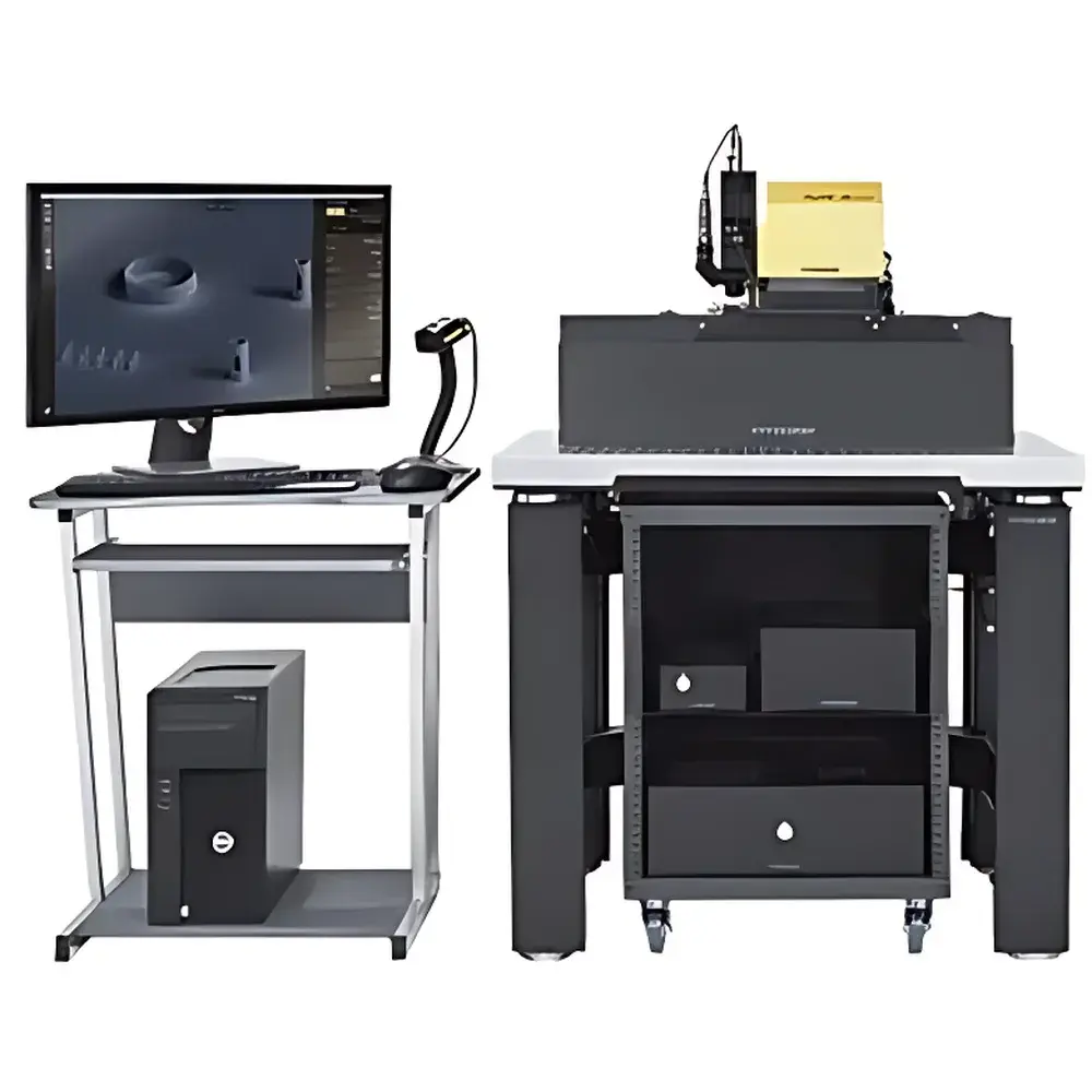
The Exaddon CERES Micro-Nano Metal 3D Printing System is a precision additive manufacturing platform engineered for direct-write fabrication of freestanding metallic microstructures with sub-micrometer spatial resolution. It operates on the principle of electrochemical deposition (ECD) mediated by FluidFM®—a proprietary technology integrating hollow atomic force microscopy (AFM) cantilevers with nanoscale fluidic control. Unlike conventional laser- or powder-based metal AM systems, CERES enables true voxel-level material placement via electrochemical reduction of metal ions at the apex of a biased, fluid-filled probe tip. This process occurs under ambient conditions (room temperature, atmospheric pressure), eliminating thermal stress, phase segregation, or post-processing requirements. The system combines high-precision piezoelectric nanopositioning (sub-5 nm resolution in X/Y/Z), real-time force feedback, and closed-loop fluid dosing to achieve deterministic growth of 3D metallic features—including overhangs, cantilevers, and interwoven architectures—without sacrificial supports. Its core capability lies in μAM (micro-additive manufacturing), positioning it uniquely at the intersection of nanofabrication, electrochemistry, and scanning probe instrumentation.
Key Features
- Sub-micrometer structural resolution: Capable of printing metallic voxels as small as 200 nm in lateral dimension and <100 nm in height.
- Support-free 3D metal printing: Enables 90° cantilevers, bridges, and suspended geometries via localized electrodeposition without scaffolding.
- FluidFM-based nanofluidic dispensing: Hollow AFM probes deliver femtoliter-to-picoliter volumes with <1 fL dosage precision per deposition event.
- Multi-material electrochemical deposition: Native support for Cu, Ag, Pt, and Au; compatible with >30 additional metal and alloy precursors (e.g., Ni, Co, Pd, Bi, Sn, and binary alloys such as Cu–Ni).
- Ambient operation: No vacuum, high temperature, or inert atmosphere required—enabling integration with optical microscopy, in situ electrical probing, or biological substrates.
- Integrated multimodal functionality: Simultaneously serves as a nanolithography tool, surface modifier, localized electrogrowth platform, and nanoscale liquid dispenser for nanoparticles (<200 nm) or functional molecules.
Sample Compatibility & Compliance
CERES accommodates conductive, semiconductive, and insulating substrates—including Si/SiO₂ wafers, ITO glass, flexible polymers (e.g., PET, PI), and biological tissues—provided an appropriate conductive seed layer (e.g., sputtered Au or Pt) is applied where necessary. All electrochemical protocols adhere to standard potentiostatic/galvanostatic control paradigms defined in ASTM E2767 and ISO 13847. The system supports GLP-compliant workflow logging, including timestamped parameter records, probe calibration history, and deposition log files traceable to individual print jobs. While not FDA-cleared as a medical device, its operational parameters align with ISO 13485 risk management principles for research-grade instrumentation used in preclinical device prototyping.
Software & Data Management
The CERES Control Suite provides a modular, scriptable environment built on Python 3.9+ with native support for Jupyter notebooks, MATLAB integration, and RESTful API access. Users define 3D structures via STL import or parametric scripting (e.g., helices, lattices, fractals), then map them to electrochemical deposition trajectories with customizable voltage ramps, dwell times, and flow rates. All experimental metadata—including environmental logs (temperature, humidity), probe deflection signals, current transients, and fluid pressure traces—are stored in HDF5 format with MIAME-compliant headers. Audit trails comply with 21 CFR Part 11 requirements for electronic records and signatures when configured with optional user-role authentication and digital certificate signing.
Applications
- Microelectromechanical systems (MEMS): Fabrication of high-aspect-ratio actuators, resonators, and compliant mechanisms with embedded electrical interconnects.
- Nanophotonics & plasmonics: Direct-write of plasmonic nanoantennas, metamaterial unit cells, and THz waveguides with sub-wavelength feature fidelity.
- Microelectronics: Repair of open circuits on ICs or PCBs; prototyping of micro-coils, RF inductors, and mmWave antennas.
- Thermal management: Additive synthesis of micro-scale heat spreaders, vapor chamber wicks, and conformal thermal interface structures.
- Biointerfaces: Site-specific metallization of neural probes, microelectrode arrays, and biohybrid scaffolds for electrochemical sensing or stimulation.
- Fundamental materials science: In situ mechanical testing of nanoscale metallic pillars, grain-boundary engineering via compositionally graded deposits, and studies of size-dependent electrochemical kinetics.
FAQ
What metals can be printed with CERES?
CERES natively supports Cu, Ag, Pt, and Au using commercially available electrolyte solutions. Over 30 additional metals—including Ni, Co, Pd, Sn, Bi, and alloy systems—are accessible through custom electrolyte formulation and protocol optimization.
Is vacuum or cleanroom operation required?
No. CERES operates under ambient laboratory conditions. A laminar flow hood or Class 1000 cleanroom is recommended for high-yield nanofabrication but not mandatory for basic functionality.
Can CERES print on non-conductive substrates?
Yes—provided a thin conductive seed layer (e.g., 5–10 nm sputtered Au or ITO) is deposited prior to printing to enable electrochemical nucleation.
What is the maximum build volume?
The standard stage offers a 100 × 100 × 20 µm³ printable volume per field of view; larger structures are achieved via automated tile stitching across multiple positions with sub-10 nm registration accuracy.
How is system calibration maintained?
CERES includes automated probe alignment routines, in situ cantilever spring constant verification, and periodic fluidic resistance calibration using reference electrolytes—documented in the instrument’s maintenance log per ISO/IEC 17025 guidelines.