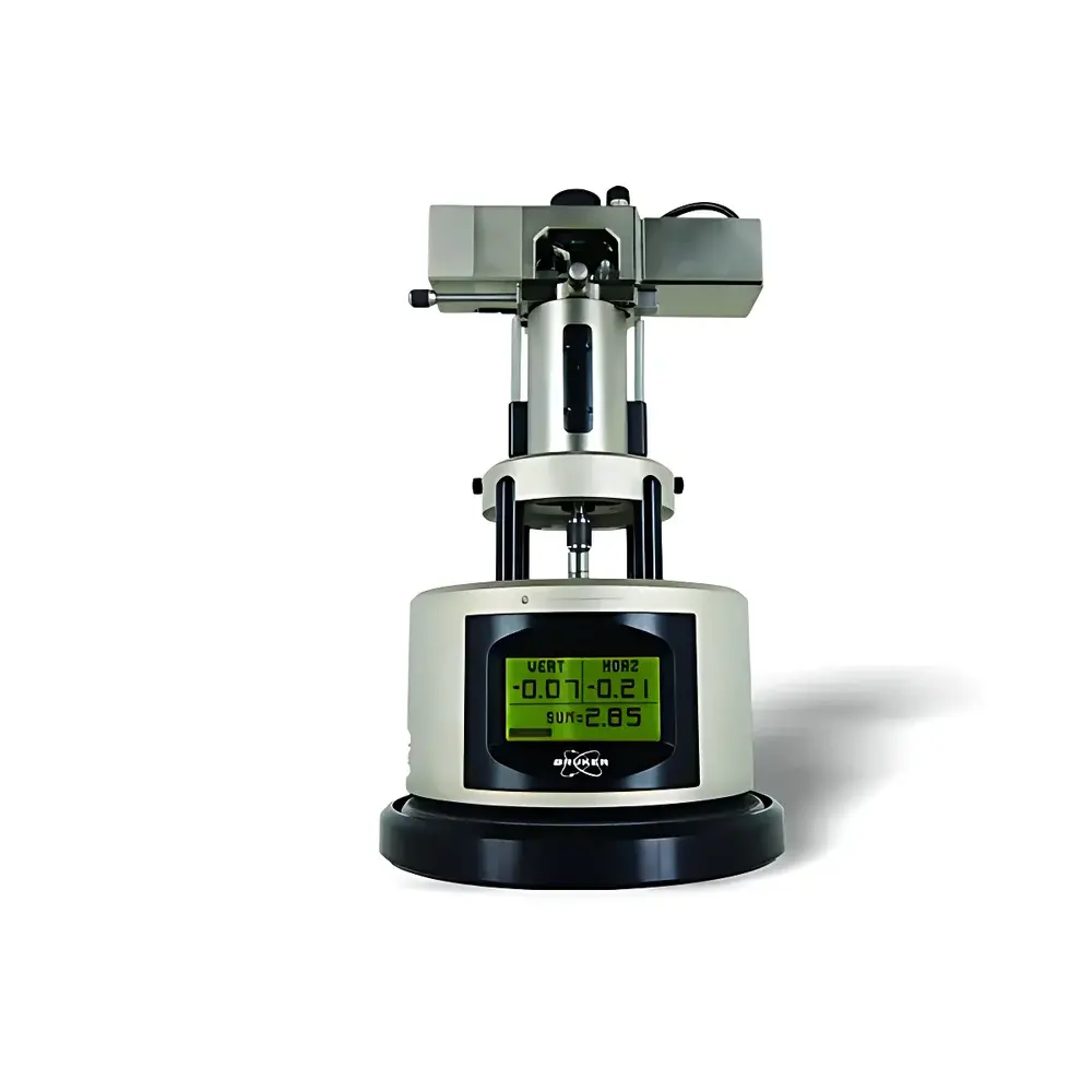
Bruker MultiMode 8 Atomic Force Microscope
| Brand | Bruker |
|---|---|
| Origin | Germany |
| Manufacturer Type | Authorized Distributor |
| Origin Category | Imported |
| Model | MultiMode 8 |
| Price Range | USD 135,000 – 205,000 |
| Instrument Type | Atomic Force Microscope (AFM) |
| Sample Dimensions | Ø15 mm × 5 mm thickness |
Overview
The Bruker MultiMode 8 Atomic Force Microscope is a high-performance scanning probe microscopy (SPM) platform engineered for nanoscale topographic, mechanical, electrical, magnetic, and thermal characterization of surfaces across diverse environments — ambient air, liquid, controlled atmosphere, and ultra-low-temperature or elevated-temperature conditions. Built upon Bruker’s decades-long legacy in AFM innovation, the MultiMode 8 integrates a rigid, low-noise mechanical architecture with the NanoScope V controller — delivering sub-angstrom height resolution, exceptional thermal and acoustic stability, and real-time force control at bandwidths exceeding 2 MHz. Its core imaging methodology relies on dynamic force modulation via PeakForce Tapping® mode, a proprietary technique that replaces conventional amplitude- or phase-based feedback with direct, cycle-by-cycle control of instantaneous tip–sample interaction force. This enables quantitative nanomechanical mapping (e.g., modulus, adhesion, deformation) simultaneously with topography — without requiring manual optimization of setpoint, gain, or scan speed.
Key Features
- PeakForce Tapping® technology: Enables piconewton-level force control (down to <50 pN), minimizing sample damage and enabling reliable imaging of soft, fragile, or hydrated biological specimens and polymers.
- PeakForce QNM® (Quantitative Nanomechanical Mapping): Delivers spatially resolved, calibrated mechanical property maps — including elastic modulus, adhesion, dissipation, and deformation — pixel-by-pixel, synchronized with topography.
- FASTForce Volume™: Accelerates 3D nanomechanical data acquisition by up to 10× compared to conventional force-volume mapping, supporting statistical analysis of heterogeneous materials.
- NanoScope V controller: Features ultra-low electronic noise floor (<0.1 nm RMS), 24-bit DAC/AAC resolution, and real-time FPGA-based processing for high-fidelity signal integrity and reproducible quantification.
- Environmental flexibility: Compatible with heating stages (up to +250 °C), cryogenic stages (down to −35 °C), and glovebox integration (H₂O/O₂ <1 ppm) for in situ studies under chemically inert or reactive atmospheres.
- ScanAsyst® automation: Eliminates resonance tuning and manual parameter adjustment; automatically optimizes probe engagement and maintains consistent tip–sample force during operation in air or liquid.
Sample Compatibility & Compliance
The MultiMode 8 accommodates standard samples up to 15 mm in diameter and 5 mm in thickness — compatible with silicon wafers, TEM grids, glass coverslips, polymer films, and electrospun membranes. Its modular design supports interchangeable scanner modules (e.g., J-scanner for high-speed imaging, E-scanner for large-area mapping) and probe holders optimized for conductive, magnetic, or thermal probes. The system complies with ISO/IEC 17025 calibration traceability requirements when operated with certified reference standards (e.g., NIST-traceable grating samples). Data acquisition and instrument control meet GLP/GMP documentation standards through optional audit-trail-enabled software configurations aligned with FDA 21 CFR Part 11 requirements.
Software & Data Management
Acquisition and analysis are performed using Bruker’s NanoScope Analysis v2.0 software suite, which provides intuitive workflow-driven interfaces for both novice and expert users. All raw force-distance curves, topographic images, and nanomechanical parameter maps are stored in vendor-neutral, metadata-rich .spm file format — fully compatible with third-party analysis tools (e.g., Gwyddion, MATLAB, Python-based SPM libraries). Batch processing scripts support automated feature extraction, statistical distribution fitting (e.g., Weibull modulus for polymer domains), and cross-correlation between mechanical and electrical channels (e.g., PFM, C-AFM). Raw data export includes ASCII, HDF5, and TIFF formats with embedded calibration parameters for full traceability.
Applications
- Materials science: Characterization of block copolymer microphase separation, graphene domain boundaries, battery electrode SEI layers, and thin-film mechanical anisotropy.
- Life sciences: High-resolution imaging of membrane proteins, DNA–protein complexes, and live-cell surface dynamics in physiological buffer — without fixation or metal coating.
- Nanoelectronics: Conductive-AFM (C-AFM) and Kelvin Probe Force Microscopy (KPFM) for local conductivity, work function, and charge trapping analysis in 2D semiconductors and perovskite solar cells.
- Polymers & composites: Quantitative modulus mapping across filler–matrix interfaces, creep/recovery behavior under nanoindentation, and environmental degradation kinetics.
- Energy research: In situ electrochemical AFM of solid electrolyte interphases (SEI) growth during Li-ion battery cycling.
FAQ
What environments can the MultiMode 8 operate in?
It functions in ambient air, liquid (including aqueous buffers and organic solvents), vacuum-compatible enclosures, temperature-controlled stages (−35 °C to +250 °C), and inert-atmosphere gloveboxes (H₂O/O₂ <1 ppm).
Is PeakForce Tapping compatible with commercial AFM probes?
Yes — it supports standard cantilevers with reflective coatings and is optimized for Bruker’s proprietary ScanAsyst-Air, ScanAsyst-Fluid, and specialized conductive/magnetic probes.
Can the system be upgraded for electrical or magnetic property mapping?
Absolutely — optional modules include Conductive AFM (C-AFM), Piezoresponse Force Microscopy (PFM), Magnetic Force Microscopy (MFM), and Scanning Thermal Microscopy (SThM), all integrated within the same software framework.
How is data integrity ensured for regulated applications?
With optional NanoScope Software Compliance Edition, the system provides electronic signatures, user access controls, change logs, and full audit trails — meeting FDA 21 CFR Part 11 and ISO 13485 requirements for quality-critical labs.
What level of technical support is provided post-installation?
Bruker-certified field application scientists deliver on-site installation, method validation, and hands-on training; remote diagnostics and firmware updates are included under annual service agreements.


