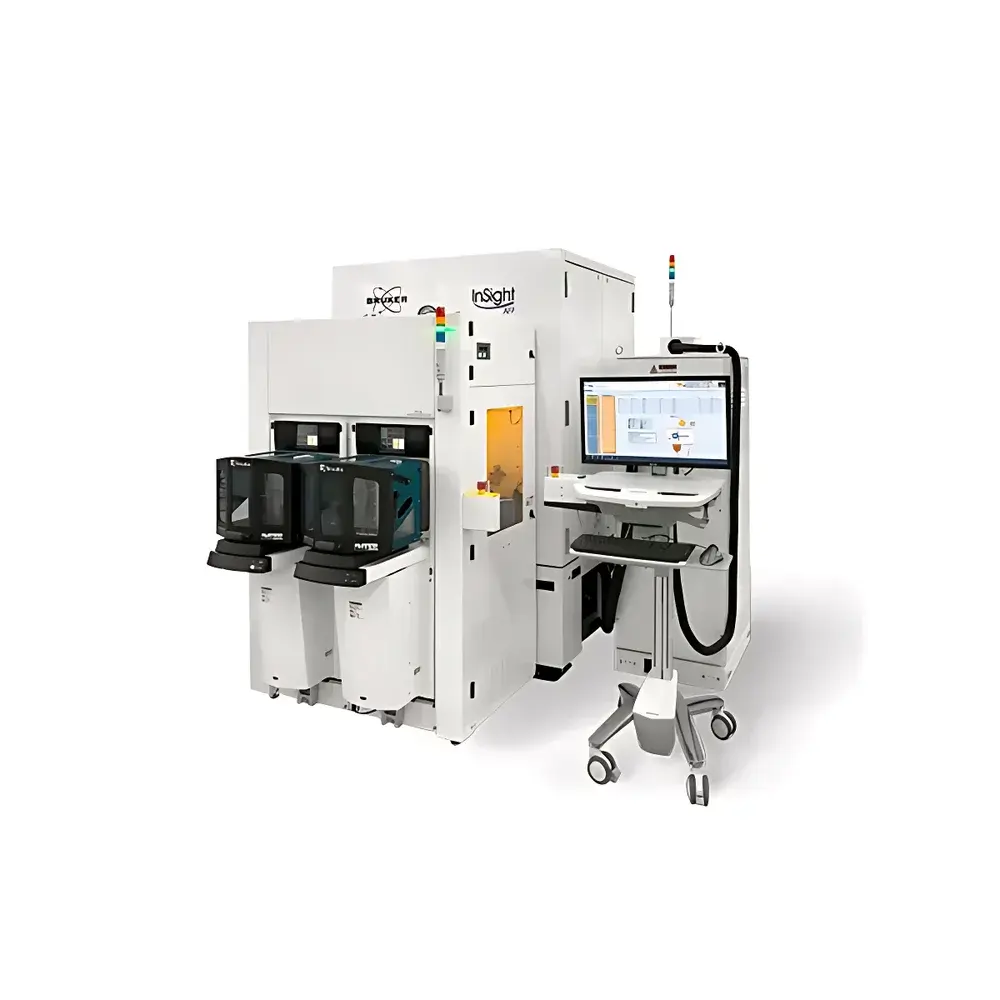
Bruker InSight AFP Automated Atomic Force Microscope
| Brand | Bruker |
|---|---|
| Origin | USA |
| Manufacturer Type | Authorized Distributor |
| Origin Category | Imported |
| Model | InSight AFP |
| Price Range | USD $2.6M–$3.2M (FOB) |
| Instrument Type | Atomic Force Microscope (AFM) |
| Application Class | Industrial Process Control System |
| XY Positioning Noise Floor | 65 nm (RMS, closed-loop) |
| Maximum Sample Size | 33 mm × 26 mm |
| Stage Travel Range | 100 mm × 300 mm (X-Y) |
| Z-Range | >2 µm (with HyperMap™ large-area stitching capability) |
| Scan Speed | Up to 36,000 µm/s (profile mode) |
| Long-Term Height Stability | <0.3 nm over 12 months (NIST-traceable calibration) |
Overview
The Bruker InSight AFP is a fifth-generation, fully automated atomic force microscope engineered for high-precision, high-throughput 3D topographic and critical dimension (CD) metrology in semiconductor manufacturing environments. Unlike conventional AFMs designed for research laboratories, the InSight AFP integrates a proprietary capacitive sensor-based force feedback system, air-bearing XY stage architecture, and TrueSense® probe motion control to deliver nanoscale resolution with industrial-grade robustness. It operates on contact-mode and dynamic-mode AFM principles—leveraging real-time tip-sample interaction detection to quantify surface morphology, step heights, sidewall angles, roughness (Ra, Rq), and etch depth without destructive cross-sectioning. Its primary application domain is post-CMP (Chemical Mechanical Polishing) and post-etch process control on 200 mm and 300 mm wafers, where it functions as an inline or offline metrology node compliant with advanced node requirements down to sub-5 nm logic and DRAM technologies.
Key Features
- TrueSense® probe actuation technology enabling sub-nanometer height repeatability and extended tip lifetime during high-speed scanning
- CDMode™ — Bruker’s proprietary AFM-based sidewall characterization mode delivering direct, model-free measurement of line edge roughness (LER), line width roughness (LWR), and sidewall angle (SWA) on patterned photoresist and hardmask layers
- HyperMap™ large-area stitching engine supporting full-field 3D mapping of standard reticle fields (33 mm × 26 mm) at pixel resolutions down to 1 µm × 1 µm, with automated hotspot detection and re-scan workflows
- Integrated high-magnification optical navigation (100× magnification) coupled with sub-250 nm global registration accuracy between optical image coordinates and AFM scan coordinates
- Automated defect review module capable of correlating topographic and phase contrast data to classify physical defects (e.g., residues, pits, bridging) and material anomalies (e.g., film delamination, particle adhesion)
- Modular design compatible with KLARITY® defect classification software and major yield management systems (YMS), including KLA, Applied Materials, and PDF Solutions platforms
Sample Compatibility & Compliance
The InSight AFP accommodates standard semiconductor substrates up to 300 mm diameter via configurable sample chucks and vacuum clamping. Its 33 mm × 26 mm maximum field-of-view supports full-reticle inspection of photomasks and stepper exposure fields. The system meets ISO/IEC 17025 requirements for calibration traceability, with NIST-traceable height standards certified annually. All measurement protocols adhere to SEMI D39 (AFM metrology guidelines), ASTM E2528 (standard practice for AFM calibration), and USP (for surface characterization in regulated pharmaceutical device manufacturing). Data integrity complies with FDA 21 CFR Part 11 through audit-trail-enabled user authentication, electronic signatures, and immutable raw data archiving.
Software & Data Management
Control and analysis are performed via Bruker’s NanoScope Analysis v3.1+ platform, featuring embedded scripting (Python API), batch processing queues, and SPC-ready statistical reporting. Measurement recipes—including scan parameters, probe selection, feedback gains, and analysis templates—are stored in encrypted XML format and version-controlled per fab lot. Raw AFM data (.spm, .wsx) and processed results (.csv, .tif) are exported directly to MES (Manufacturing Execution Systems) via SECS/GEM protocol or RESTful API integration. All measurement logs include timestamped metadata (operator ID, environmental conditions, calibration status) required for GLP/GMP audits.
Applications
- Post-CMP dishing and erosion quantification across die-level interconnect structures (Cu/low-k, Co/Ru, Ru liner stacks)
- Etch depth uniformity mapping for FinFET, GAA, and memory trench structures
- Photomask defect root-cause analysis using simultaneous topography + phase imaging
- Hardmask integrity assessment following selective etch processes (e.g., SiN, SiO₂, TiN)
- 3D packaging metrology: microbump height, solder joint coplanarity, and underfill void detection
- Advanced packaging R&D: TSV (Through-Silicon Via) sidewall roughness and conformality evaluation
FAQ
What wafer sizes does the InSight AFP support?
The system is configured for 200 mm and 300 mm wafers, with optional adaptors for smaller substrates (e.g., 150 mm, SOI, compound semiconductors).
Is CDMode™ compatible with all probe types?
CDMode requires Bruker’s proprietary CD-AFM probes (e.g., RTESPA-CD, SCANASYST-CD), optimized for sidewall contact stability and minimal tip wear during vertical profiling.
How is long-term measurement stability validated?
Bruker provides annual NIST-traceable height calibration using SRM 2164 (step-height standard), with in-house drift monitoring logs archived for regulatory review.
Can the InSight AFP integrate into existing factory automation?
Yes — it supports SECS/GEM communication, CIM (Computer Integrated Manufacturing) interfaces, and robotic handler compatibility (e.g., Brooks, MKS, Asyst) via standard SMIF/FOUP load ports.
What is the typical throughput for full-field 3D mapping?
At 1 µm × 1 µm pixel resolution over a 33 mm × 26 mm field, full acquisition and hotspot re-scan completes within 24 hours; higher-speed modes (e.g., 5 µm × 5 µm) achieve full-field coverage in under 2 hours.


