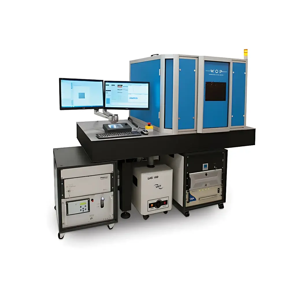
Workshop of Photonics Femto LAB Femtosecond Laser Micro-Nanofabrication System
| Brand | Workshop of Photonics (WOP, Lithuania) |
|---|---|
| Model | Femto LAB |
| Origin | Lithuania |
| Laser Pulse Duration | <150 fs |
| Maximum Repetition Rate | Up to 1 MHz (configurable) |
| Wavelength | 1030 nm (fundamental), optionally frequency-doubled to 515 nm |
| Spot Size (diffraction-limited) | <300 nm (at 1030 nm, with high-NA objective) |
| Positioning Resolution | <10 nm (closed-loop piezo stages) |
| Layer-to-Layer Alignment Accuracy | ±20 nm |
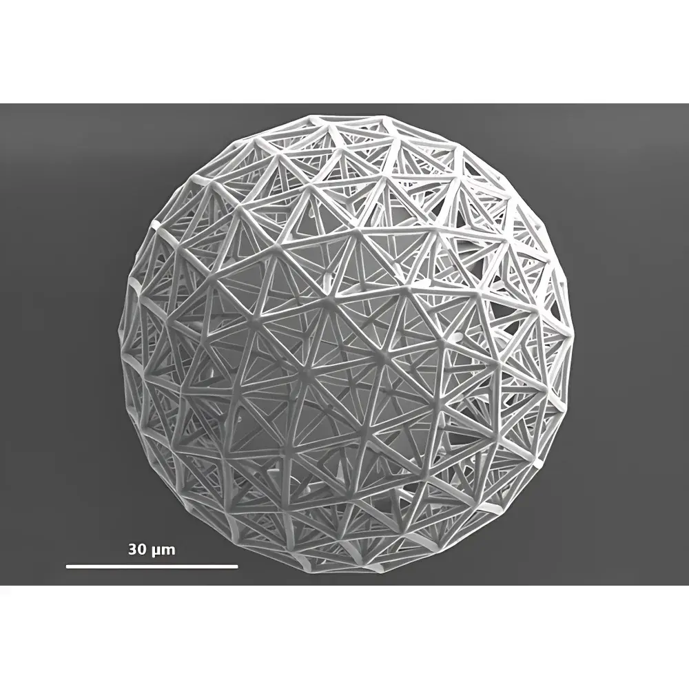
| Minimum Feature Size | 100 nm (via multiphoton polymerization) |
| Compatible Materials | Photoresists (e.g., IP-L 780, SZ2080, OrmoComp), sol-gel glasses, fused silica, silicon, metals (via ablation) |
| Software Platform | SCA Microfabrication Suite (v5.2+) with Python API, GLP-compliant audit trail, and optional machine vision integration |
| Compliance | CE marked, ISO 13849-1 PL e safety architecture, compatible with ISO/IEC 17025 laboratory accreditation workflows |
Overview
The Workshop of Photonics Femto LAB is a turnkey femtosecond laser micro-nanofabrication system engineered for high-precision, maskless, three-dimensional structuring of transparent and reflective materials at sub-100 nm resolution. Based on the principle of nonlinear multiphoton absorption, the system enables true 3D lithography inside bulk dielectrics—without thermal damage or collateral modification—by tightly focusing ultrashort (<150 fs), high-peak-power laser pulses into photosensitive media. Unlike conventional UV photolithography or two-photon polymerization (TPP) systems limited to planar or low-aspect-ratio structures, the Femto LAB supports both additive (e.g., direct laser writing via multiphoton polymerization) and subtractive (e.g., femtosecond laser ablation, trenching, drilling) modalities within a single integrated platform. Its modular optical architecture accommodates interchangeable objectives (up to 100×, NA ≥ 1.4), motorized sample stages with closed-loop nanometer positioning, and real-time beam diagnostics—making it suitable for academic research, photonics prototyping, and pre-GMP microdevice development.
Key Features
- Ultrafast Laser Source: Industrial-grade Yb-based fiber amplifier delivering <150 fs pulses at 1030 nm (optionally 515 nm via SHG), with repetition rates tunable from single-shot to 1 MHz, enabling precise energy deposition control per voxel.
- Nanopositioning & Metrology: High-stiffness piezoelectric XYZ stages with interferometric feedback, achieving <10 nm open-loop repeatability and ±20 nm layer registration accuracy—critical for multilayer photonic crystal or microfluidic device fabrication.
- Adaptive Beam Delivery: Galvo-scanning combined with high-NA objective optics and dynamic wavefront correction (optional deformable mirror) ensures diffraction-limited focus stability across extended scan fields (>100 × 100 µm²).
- Material-Agnostic Processing: Optimized for photoresists (IP-L 780, SZ2080), hybrid organic-inorganic sol-gels, fused silica, crystalline silicon, and thin metal films—enabling hybrid integration of optical, mechanical, and electronic functionalities.
- SCA Microfabrication Software: Graphical user interface with vector-based path planning, voxel-by-voxel exposure control, batch job queuing, and full parameter logging. Supports Python scripting for custom workflow automation and integration with external metrology tools (e.g., SEM, AFM).
Sample Compatibility & Compliance
The Femto LAB processes substrates up to 100 mm in diameter and 25 mm thick—including wafers, microscope slides, optical fibers, and flexible polymer foils. Sample holders are configurable for vacuum clamping, magnetic fixation, or kinematic alignment. All hardware and software components comply with CE directives for machinery safety (EN ISO 13849-1, Performance Level e) and electromagnetic compatibility (EN 61326-1). The SCA software supports audit-trail generation, user access levels, and electronic signature capability—aligning with ISO/IEC 17025 requirements for accredited testing laboratories and facilitating future FDA 21 CFR Part 11 readiness when deployed in regulated R&D environments.
Software & Data Management
SCA Microfabrication Suite (v5.2+) serves as the central control environment. It records every fabrication event—including laser pulse count, stage coordinates, power calibration timestamp, and environmental sensor data (temperature, humidity)—in encrypted SQLite databases with SHA-256 checksums. Raw log files are exportable in CSV/JSON format for traceability. Optional modules include automatic focus tracking (via confocal reflectance or interferometric focus sensing), real-time machine vision-based defect detection (using OpenCV pipelines), and bidirectional synchronization with CAD/CAM platforms (STEP, GDSII import/export). All software updates undergo version-controlled release validation and are distributed via secure HTTPS repositories.
Applications
- Photonic crystals and metamaterials with bandgap engineering down to visible wavelengths
- Micro-optical elements: freeform microlenses, diffractive optical elements (DOEs), and geometric phase plates fabricated directly in fused silica
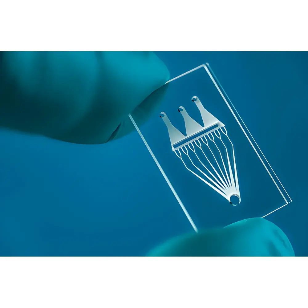
- Lab-on-chip devices: monolithic 3D microfluidic networks with embedded valves, mixers, and optical waveguides
- Bio-integrated scaffolds: silk fibroin and gelatin methacryloyl (GelMA) microarchitectures with subcellular feature fidelity
- Microelectromechanical systems (MEMS): freestanding cantilevers, resonators, and actuators in doped silicon or nickel
- Calibration standards: NIST-traceable line gratings, step-height artifacts, and atomic force microscopy (AFM) tip sharpening templates
FAQ
What is the minimum achievable feature size in multiphoton polymerization mode?
The system achieves consistent 100 nm line widths in IP-L 780 under optimized exposure conditions (pulse energy ~20 nJ, repetition rate 200 kHz, 100× oil-immersion objective). Sub-50 nm features have been demonstrated in peer-reviewed publications using customized processing protocols.
Can the Femto LAB process conductive or metallic materials?
Yes—through femtosecond laser ablation, the system fabricates high-fidelity microstructures in gold, aluminum, titanium, and ITO thin films without delamination or recast layer formation. Ablation thresholds and debris mitigation strategies are pre-characterized for common PVD- and sputter-deposited layers.
Is remote operation and monitoring supported?
The SCA software includes a secure WebSocket-based remote interface (TLS 1.3 encrypted), allowing real-time status monitoring, job queue management, and emergency stop initiation from off-site locations—fully auditable within the system’s event log.
How is laser power calibrated and maintained over time?
An integrated pyroelectric sensor with NIST-traceable calibration certificate measures average power before each job. Pulse energy is inferred via repetition rate and monitored continuously using a fast photodiode; deviations >±2% trigger an automatic recalibration sequence.
Does the system support multi-material or hybrid fabrication workflows?
Yes—sequential processing is enabled by programmable stage repositioning, automated sample exchange (with optional robotic loader), and material-specific exposure recipes stored in the SCA database. Published work includes silica-on-silicon photonic circuits with embedded polymer waveguides and metal interconnects.


