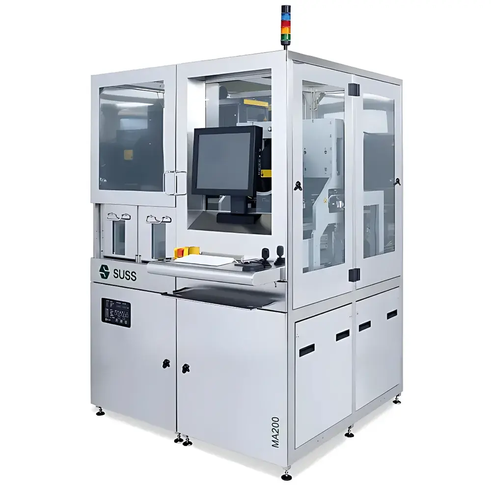
SUSS MA200 Gen3 Fully Automated Mask Aligner
| Brand | SUSS |
|---|---|
| Origin | Germany |
| Model | MA200 Gen3 |
| Substrate Compatibility | ≤200 mm wafers & square substrates |
| Alignment Accuracy (Top-Side) | ≤0.5 µm |
| Resolution (Vacuum Contact Mode) | <0.8 µm |
| Resolution (Proximity Mode) | ≥3.5 µm |
| Exposure Optics | MO Exposure Optics® with telecentric illumination, HR/LGO mode switching, customizable filters & reduction kits for smaller wafers |
| Automation Level | Fully automated batch processing |
| Compliance | Designed for ISO Class 5–7 cleanroom integration, compatible with SEMI S2/S8 safety standards and GLP/GMP-aligned process documentation workflows |
Overview
The SUSS MA200 Gen3 Fully Automated Mask Aligner is a high-precision photolithography tool engineered for volume manufacturing of microstructures on substrates up to 200 mm in diameter or square format. It operates on the principle of contact and proximity photolithography—where UV light is projected through a photomask onto a photosensitive resist layer—and integrates advanced alignment metrology, adaptive illumination, and deterministic automation to meet stringent requirements in MEMS, RF devices, power semiconductors, image sensors, and advanced packaging (e.g., fan-out wafer-level packaging, bumping, 3D integration). Unlike stepper-based systems, the MA200 Gen3 delivers cost-effective, mask-based patterning with sub-micron overlay control, making it particularly suited for prototyping-to-production transitions and applications where mask fidelity, process stability, and rapid reconfiguration are critical.
Key Features
- DirectAlign® with PatMax Vision: Real-time, pattern-agnostic top-side alignment using live camera imaging—eliminating reliance on stored reference templates—enabling ≤0.5 µm overlay accuracy with high repeatability across wafer lots.
- MO Exposure Optics®: Modular, telecentric illumination system delivering uniform irradiance (±2% across field) and thermal stability; supports rapid switching between High-Resolution (HR) and Low-Glare Optimization (LGO) modes without hardware recalibration.
- Multi-Mode Exposure Capability: Configurable operation in proximity (≥3.5 µm resolution), soft/hard contact, and vacuum contact modes—with verified sub-0.8 µm resolution under vacuum contact conditions—ensuring adaptability across R&D, pilot line, and high-mix production environments.
- Fragile Substrate Handling: Interchangeable chuck modules and edge-handling carriers accommodate warped, ultra-thin (down to 50 µm), or double-sided structured wafers while maintaining mechanical integrity and minimizing particle generation.
- Field-Configurable Optics: Plug-and-play filter sets (i-line, g-line, broadband) and optional reduction optics kits enable seamless adaptation to smaller substrates (e.g., 100 mm, 150 mm) without sacrificing optical performance or alignment fidelity.
Sample Compatibility & Compliance
The MA200 Gen3 supports silicon, glass, quartz, sapphire, and compound semiconductor substrates (e.g., GaAs, SiC, InP) ranging from 50 µm to 200 mm in diameter or equivalent square dimensions. Its vacuum chuck, electrostatic clamping options, and programmable gap control ensure reliable adhesion and minimal stress transfer during exposure. The system is designed for integration into ISO Class 5–7 cleanrooms and conforms to SEMI S2 (safety) and S8 (ergonomics) standards. Process logs—including alignment coordinates, exposure dose, lamp intensity, vacuum pressure, and stage positioning—are timestamped and exportable in CSV/Excel formats, supporting traceability requirements under GLP and GMP frameworks. While not inherently 21 CFR Part 11-compliant, its audit trail architecture allows integration with third-party electronic lab notebook (ELN) or MES platforms for regulated environments.
Software & Data Management
The MA200 Gen3 runs on SUSS’ proprietary AutoAlign™ software suite, featuring intuitive recipe-driven operation, multi-layer alignment sequence programming, and real-time alignment deviation feedback. All alignment data—including fiducial detection confidence scores, pixel displacement vectors, and correction offsets—are stored per wafer and accessible via the embedded SQL database. Export functions support standardized metadata tagging (e.g., wafer ID, lot number, operator ID, timestamp) and can be configured to push data to factory-level SCADA or MES systems via OPC UA or REST API interfaces. Software updates are delivered via secure offline packages to maintain system validation integrity in controlled manufacturing settings.
Applications
- MEMS fabrication requiring high-fidelity replication of deep etch structures and movable elements
- RF front-end module patterning on high-resistivity silicon or GaAs substrates
- Advanced packaging processes including redistribution layer (RDL) formation, copper pillar bumping, and TSV passivation
- Image sensor backside illumination (BSI) processing with double-sided alignment and thin-wafer handling
- Compound semiconductor device manufacturing (e.g., HEMTs, photodiodes) demanding low-defect, low-stress lithography
- Research and development of novel 3D interconnect architectures and heterogeneous integration schemes
FAQ
What substrate sizes does the MA200 Gen3 support?
The system handles round wafers up to 200 mm and square substrates up to 156 mm × 156 mm, with optional reduction kits enabling full-field exposure on smaller formats (e.g., 100 mm, 150 mm).
Is vacuum contact mode required to achieve sub-0.8 µm resolution?
Yes—sub-0.8 µm resolution is validated only in vacuum contact mode; proximity mode resolution is limited to ≥3.5 µm due to diffraction-limited gap constraints.
Can the MA200 Gen3 be integrated into an automated material handling system (AMHS)?
It supports SECS/GEM communication protocols and includes standard FOUP/FOSB load port interfaces compatible with most 200 mm AMHS configurations.
Does the system support double-sided alignment?
Yes—via optional dual-camera configuration and through-wafer alignment capability using infrared-transparent substrates or alignment marks on both sides.
How is process reproducibility ensured across shifts and operators?
Through recipe locking, user-role-based access control, automated calibration routines (e.g., illumination uniformity mapping, stage encoder verification), and immutable process log archiving.


