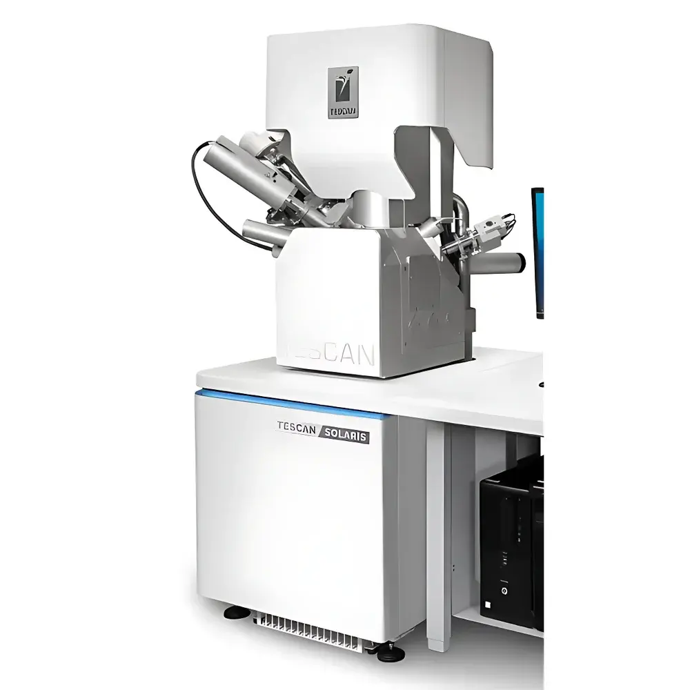
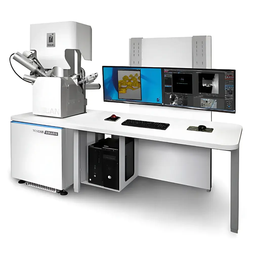
TESCAN SOLARIS Ga⁺ Focused Ion Beam-Scanning Electron Microscope (FIB-SEM)
| Brand | TESCAN |
|---|---|
| Origin | Czech Republic |
| Model | TESCAN SOLARIS |
| Ion Source | Liquid Metal Gallium (Ga⁺) |
| SEM Column | Triglav™ High-Resolution Field Emission SEM |
| FIB Column | Orage™ High-Current Ga⁺ FIB |
| Maximum Ion Beam Current | 100 nA |
| Minimum FIB Acceleration Voltage | 500 V |
| In-Column Detector System | Energy-Filtered Axial Backscattered Electron (BSE) Detection |
| Integrated GIS | Up to 3 OptiGIS™ or 5-Nozzle Coaxial Gas Injection Systems |
| Software Platform | TESCAN Essence™ with DrawBeam™ Vector-Based Milling Engine |
| Sample Chamber | Ultra-Large, Optimized for 6″–8″ Wafers |
| Electron Beam Current | Up to 400 nA (Schottky Field Emission Gun) |
| Compliance | Designed for GLP/GMP environments |
Overview
The TESCAN SOLARIS is a high-performance dual-beam focused ion beam–scanning electron microscope (FIB-SEM) engineered for demanding nanoscale characterization, precision sample preparation, and advanced in situ nanofabrication. Built around two purpose-designed, co-aligned columns — the Triglav™ high-resolution field-emission SEM and the Orage™ high-current gallium-ion FIB — the system delivers exceptional imaging fidelity, sub-20 nm TEM lamella preparation capability, and robust large-volume milling performance. Its core operational principle combines high-efficiency electron signal detection with energy-filtered axial backscattered electron (BSE) collection, enabling simultaneous topographic and compositional contrast at low kV without charge accumulation. The Ga⁺ ion column operates across a wide voltage range (500 V–30 kV), allowing controlled sputtering, final polishing, and minimal subsurface damage — critical for preparing artifact-free transmission electron microscopy (TEM) specimens, EBSD-ready surfaces, and ultra-thin semiconductor cross-sections. The system’s architecture integrates hardware-level stability (e.g., piezo-driven aperture changers, ultra-stable high-voltage supplies) with software-defined workflows, making it suitable for both routine industrial metrology and exploratory academic research.
Key Features
- Triglav™ SEM column featuring in-column energy-filtered BSE detection — delivering >3× higher signal efficiency and enhanced surface sensitivity, especially below 5 kV
- Orage™ Ga⁺ FIB column with continuous beam current range from <1 pA to 100 nA and acceleration voltage down to 500 V — enabling both ultra-fine nanomachining and rapid bulk removal
- Optimized 60° objective lens geometry and ultra-large chamber accommodating full 8-inch wafers with unobstructed access to edge and center positions
- Up to three independent OptiGIS™ gas injection systems or a 5-nozzle coaxial GIS — supporting Pt/C deposition, XeF₂ etching, and site-specific passivation
- TESCAN Essence™ software platform with modular layout manager, application-specific wizards (e.g., AutoLamella, AutoEBSD), and DrawBeam™ vector-based milling engine for sub-pixel beam placement accuracy
- Schottky field-emission electron source delivering up to 400 nA beam current with fast kV switching — ensuring optimal conditions for EDS, WDS, and EBSD acquisition during or after FIB processing
Sample Compatibility & Compliance
The TESCAN SOLARIS accommodates diverse sample types — from insulating biological tissues and polymer composites to conductive semiconductor wafers and ceramic thin films — without mandatory metal coating, thanks to integrated beam-induced charge neutralization and low-kV imaging optimization. Its large chamber design supports standard SEM stubs, TEM grids, lift-out needles, and full-diameter wafers (up to 200 mm). All critical instrument parameters — including beam settings, GIS gas selection, stage coordinates, and detector configurations — are logged with timestamped metadata and user attribution, satisfying traceability requirements under ISO/IEC 17025, ASTM E1558, and FDA 21 CFR Part 11. Optional audit trail modules support GLP/GMP-compliant laboratories conducting failure analysis, process validation, or regulatory submissions.
Software & Data Management
TESCAN Essence™ serves as the unified interface for acquisition, processing, and automation. Its layout manager allows persistent workspace customization per user role (e.g., operator, analyst, supervisor), while the built-in scripting engine (Python API) enables integration with external data pipelines and laboratory information management systems (LIMS). Automated workflows — such as sequential lamella milling, slice-and-view tomography, and EBSD pattern indexing — reduce manual intervention and improve inter-user reproducibility. All acquired images, spectra, and stage trajectories are stored in vendor-neutral HDF5 format with embedded calibration metadata, facilitating long-term archival and third-party reconstruction (e.g., Avizo, Dragonfly). Real-time 3D volume rendering and on-the-fly EDS/EBSD correlation are supported during FIB-SEM serial sectioning.
Applications
- High-yield preparation of electron-transparent TEM lamellae from advanced nodes (<5 nm logic, 3D NAND, GAA transistors), with final polish at ≤1 kV minimizing amorphization
- Site-specific cross-sectioning and trenching of packaged ICs for fault isolation and process verification
- 3D nanostructural reconstruction via FIB-SEM tomography, combined with simultaneous EDS elemental mapping and EBSD crystallographic orientation analysis
- In situ nanomechanical testing using microfabricated cantilevers or TEM-compatible MEMS devices
- Preparation of EBSD-optimized surfaces on grain-boundary-sensitive materials (e.g., Ni-based superalloys, battery cathodes)
- Gas-assisted nanofabrication of plasmonic structures, photonic crystals, and quantum dot arrays using DrawBeam™ vector patterning
FAQ
What is the minimum achievable TEM lamella thickness using the TESCAN SOLARIS?
Typical final lamellae thickness ranges from 20 nm to 50 nm, depending on material hardness and final polishing voltage. Sub-20 nm thicknesses have been demonstrated on Si and SiO₂ with optimized low-kV (<1 kV) final polish protocols.
Can the system perform automated serial sectioning for 3D reconstruction?
Yes — the Essence™ software includes a dedicated Slice-and-View module with real-time drift correction, auto-focus, and adaptive slice thickness adjustment based on signal-to-noise feedback.
Is the Orage™ FIB column compatible with cryogenic stages?
The SOLARIS platform supports optional cryo-transfer and cryo-stage integration for temperature-controlled FIB-SEM work on beam-sensitive biological or organic samples.
How does the Triglav™ column achieve improved surface sensitivity at low kV?
Through its in-column energy-filtered axial BSE detector, which selectively collects low-loss BSE signals — enhancing atomic-number contrast while suppressing topographic artifacts common in conventional in-lens detectors.
Does the system support correlative light and electron microscopy (CLEM)?
Yes — the large chamber and precise coordinate referencing enable integration with optical modules (e.g., fluorescence stage inserts), and Essence™ supports overlay of confocal or super-resolution optical maps onto FIB-SEM volumes.


