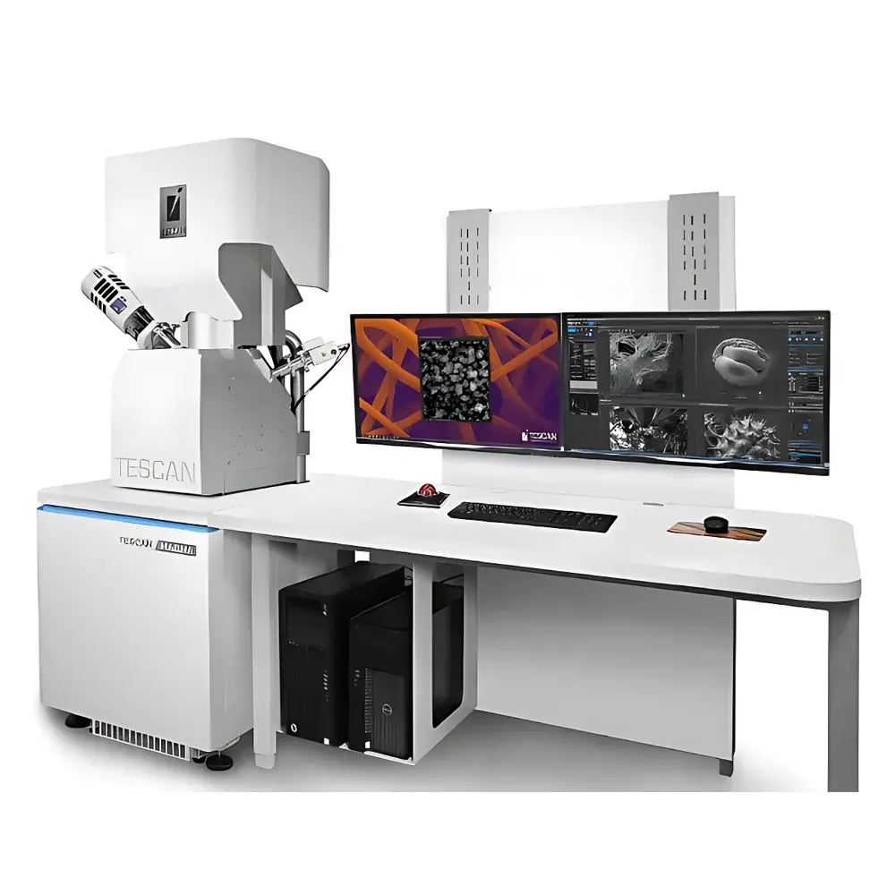
TESCAN MAGNA Field Emission Scanning Electron Microscope
| Brand | TESCAN |
|---|---|
| Origin | Czech Republic |
| Instrument Type | Floor-standing SEM |
| Electron Gun | Schottky Field Emission |
| Secondary Electron Resolution | 0.6 nm @ 15 kV |
| Magnification Range | 7× to 2,000,000× |
| Accelerating Voltage | 200 V – 30 kV (reduced to 50 V in deceleration mode) |
| Backscattered Electron Resolution | 1.6 nm @ 15 kV |
Overview
The TESCAN MAGNA is a high-performance field emission scanning electron microscope (FE-SEM) engineered for nanoscale characterization with exceptional resolution, signal fidelity, and analytical versatility. Built around the proprietary Triglav™ SEM column—a tri-lens optical architecture—the MAGNA delivers sub-nanometer resolution at both high and low accelerating voltages, enabling reliable imaging of beam-sensitive, non-conductive, and magnetic materials without conductive coating. Its core measurement principle relies on focused electron beam–sample interactions, generating secondary electrons (SE), backscattered electrons (BSE), and characteristic X-rays for morphological, compositional, and crystallographic analysis. Designed for demanding research and industrial QA/QC environments—including semiconductor metrology, advanced materials development, and life sciences—the MAGNA meets the stringent requirements of modern nanotechnology laboratories where surface sensitivity, low-voltage performance, and multi-modal signal acquisition are critical.
Key Features
- Triglav™ Tri-Lens Column Architecture: Integrates three independently optimized objective lenses—UH-resolution lens for sub-0.6 nm imaging, Analytical lens with zero magnetic field at the sample for EDS/EBSD of magnetic specimens, and Multi-Mode lens for dynamic beam shaping and working distance flexibility.
- TriBE™ & TriSE™ Detector Systems: Three-angle BSE detection (in-column mid-angle, in-beam forward-BSE, and chamber-mounted wide-angle) enables atomic-number-, topography-, and channeling-contrast imaging. Triple SE detection (in-beam SE, BDM-mode SE, and chamber SE) ensures optimal signal yield across all operating conditions, including ultra-low kV and short working distances.
- Schottky Field Emission Source: Delivers stable, high-brightness electron beams with current up to 400 nA and rapid voltage switching (<100 ms), supporting high-speed mapping, quantitative EDS, and time-resolved analysis.
- Enhanced Signal Detection Efficiency: Optimized in-column detector geometry increases SE/BSE collection efficiency by >3× versus prior-generation columns; energy-filtered axial BSE detection improves surface sensitivity and material contrast at low kV.
- Adaptive Probe Optimization: Real-time beam convergence control maintains optimal probe size and current across magnifications and kV settings—critical for high-fidelity EDS, WDS, and EBSD quantification.
Sample Compatibility & Compliance
The MAGNA excels in imaging uncoated, insulating, and beam-sensitive samples—including ceramics, polymers, biological tissues, photoresists, and perovskite thin films—without charging artifacts, thanks to its robust low-kV (down to 50 V) imaging capability and active charge compensation. The system supports standard 3-inch and 4-inch wafers, bulk specimens up to 150 mm diameter, and specialized holders for in-situ heating, cooling, or electrical biasing. It complies with ISO 16700:2016 (SEM measurement uncertainty), ASTM E1558 (SEM imaging practice), and supports GLP/GMP workflows through audit-trail-enabled software logging. Optional integration with EDAX, Oxford Instruments, or Bruker detectors ensures full compatibility with ISO 14789, ASTM E1508, and IEC 62232 for elemental and phase analysis.
Software & Data Management
TESCAN Essence™ is a modular, role-based software platform built on a Qt-based framework and compliant with FDA 21 CFR Part 11 requirements for electronic records and signatures. Its Layout Manager allows fully customizable UI configurations per user profile or application domain (e.g., failure analysis, particle metrology, or life science). Automated workflows include SmartAlign (auto-stigmation/focus), AutoTune (beam optimization), and ScriptRunner for batch processing. All acquisitions embed metadata (kV, WD, dwell time, detector settings, stage coordinates) in TIFF/OME-TIFF format. Raw data export supports HDF5 and MRC standards; integration with Python (via TESCAN SDK) enables custom image processing, AI-assisted segmentation, and LIMS connectivity.
Applications
- Nanomaterial morphology and defect analysis (carbon nanotubes, MXenes, quantum dots)
- High-resolution semiconductor metrology: gate oxide thickness, trench profiles, EUV resist characterization
- Uncoated biological ultrastructure imaging (cryo-fixed cells, collagen fibrils, neural tissue)
- Magnetic domain imaging via BSE channeling contrast and EBSD orientation mapping
- In-situ thermal/electrical testing with real-time SE/BSE correlation
- Automated particle analysis (size, shape, composition) per ISO 13322-2 and ASTM E1245
FAQ
What is the minimum working distance required for optimal resolution at 1 kV?
The Triglav™ column achieves best-in-class low-kV resolution at working distances as short as 1.5 mm using the In-Beam SE detector.
Can the MAGNA perform simultaneous EDS and EBSD acquisition?
Yes—its zero-field Analytical lens and synchronized detector triggering enable concurrent, spatially registered EDS and EBSD mapping without signal interference.
Is remote operation supported for multi-user labs?
Essence™ includes secure web-based remote desktop access with session logging, user-level permissions, and real-time collaboration tools.
How does the system handle charging on insulating samples?
Through combined use of low-kV imaging (50–1 kV), beam deceleration mode, and optional low-vacuum or gas injection options (e.g., water vapor), minimizing surface potential buildup.
What calibration standards are traceable for metrology applications?
TESCAN provides NIST-traceable grating standards (e.g., PTB 0100 series) and certifies resolution performance per ISO 16700 Annex C protocols.


