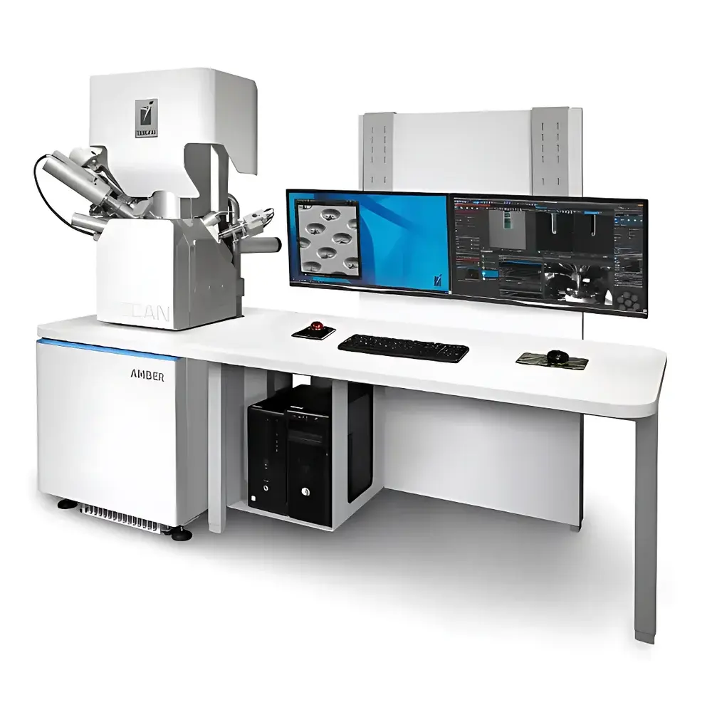
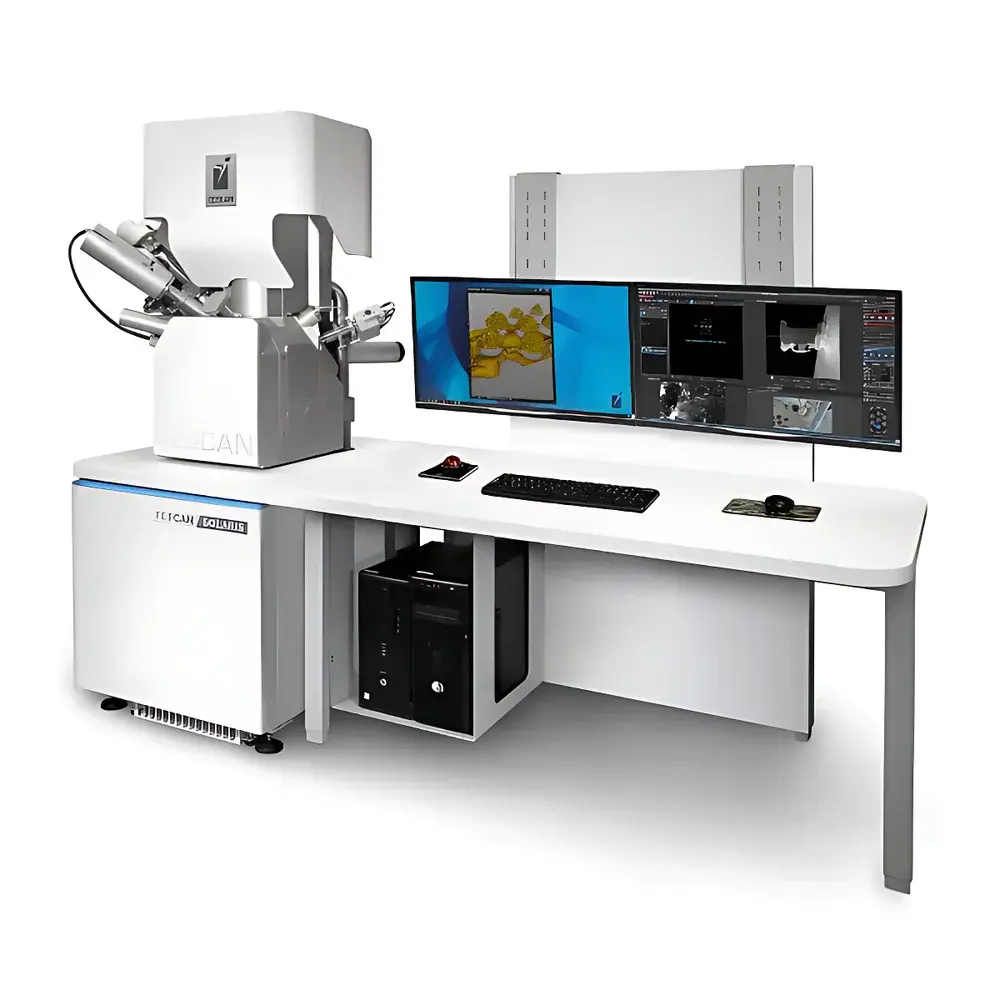
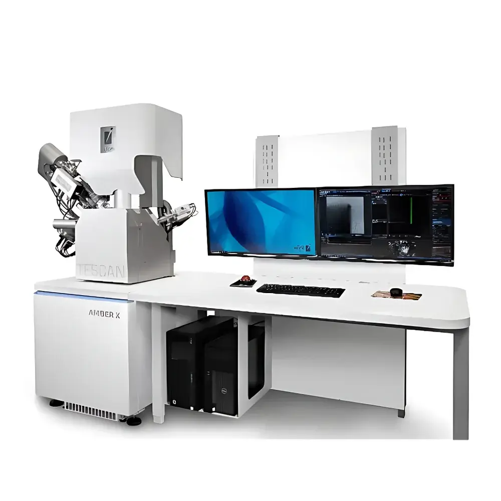
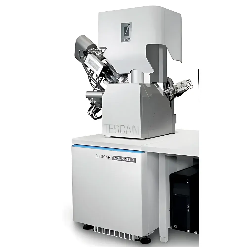
TESCAN FIB-SEM Dual-Beam Scanning Electron Microscope (Amber / Solaris Series)
| Brand | TESCAN |
|---|---|
| Origin | Czech Republic |
| Model Series | AMBER, SOLARIS, AMBER X, SOLARIS X |
| Ion Sources | Liquid Metal Ga⁺ & Plasma Xe⁺ |
| Resolution (Xe-FIB) | <15 nm |
| Beam Alignment | Co-located Electron/Ion Optical Axes |
| System Architecture | Integrated UHV Dual-Column Platform |
Overview
The TESCAN FIB-SEM Dual-Beam Scanning Electron Microscope represents a fully integrated ultra-high vacuum (UHV) platform combining high-resolution field-emission scanning electron microscopy (FE-SEM) with focused ion beam (FIB) milling, deposition, and imaging capabilities. Engineered for nanoscale characterization and in situ fabrication, this system operates on the principle of coincident electron and ion optical axes—ensuring precise spatial registration between SEM imaging and FIB manipulation. The dual-beam architecture enables real-time monitoring of ion-induced material modification (e.g., cross-sectioning, trenching, lamella preparation) at sub-15 nm resolution, eliminating iterative alignment and significantly reducing operational uncertainty. Unlike standalone SEM or FIB tools, the co-located beam design supports deterministic nanofabrication workflows essential for semiconductor failure analysis, TEM sample preparation, 3D tomography, and materials science research under GLP-compliant laboratory conditions.
Key Features
- Co-axial beam alignment with sub-micron overlap tolerance between FE-SEM and FIB columns, enabling true simultaneous imaging and milling.
- Dual ion source options: High-brightness liquid metal gallium (Ga⁺) source for sub-5 nm precision milling and nanoscale circuit edit; high-current xenon plasma (Xe⁺) source delivering >50× higher sputter rate than Ga⁺ while maintaining <15 nm probe resolution.
- Advanced stage metrology with 5-axis motorized precision stage (±0.1 µm repeatability), integrated laser interferometry for positional feedback, and tilt range up to ±90° for oblique-angle milling and tomographic acquisition.
- Multi-detector SEM configuration including in-lens SE, BSE, STEM, and energy-filtered backscattered electron (EF-BSE) detectors for compositional and crystallographic contrast.
- On-board gas injection systems (GIS) supporting Pt, C, and W deposition, as well as selective etching (e.g., I₂, XeF₂) for contamination-free processing in semiconductor and MEMS applications.
- Modular vacuum architecture with differential pumping stages ensuring stable base pressure ≤1×10⁻⁸ mbar in the sample chamber during extended FIB operation.
Sample Compatibility & Compliance
The TESCAN FIB-SEM accommodates conductive and non-conductive specimens up to 150 mm in diameter (standard configuration), with optional large-chamber variants supporting wafers up to 300 mm. Conductive coating is not required for most insulating samples due to low-voltage SEM imaging (0.1–30 kV) and beam-induced charge compensation via flood gun. All systems comply with CE marking requirements, ISO 14644-1 Class 5 cleanroom compatibility, and meet electromagnetic compatibility (EMC) standards per EN 61326-1. For regulated environments—including semiconductor fabs and pharmaceutical R&D labs—the platform supports audit-ready operation with optional 21 CFR Part 11–compliant software modules, electronic signatures, and full audit trail logging for all instrument parameters, user actions, and image metadata.
Software & Data Management
TESCAN’s proprietary iQ+ software suite provides unified control of both electron and ion beams through a single graphical interface. Workflow automation includes scriptable protocols for serial sectioning (SBF-SEM), automated lamella lift-out, and multi-region FIB milling with position referencing across sessions. Image data is stored in vendor-neutral TIFF/OME-TIFF formats compliant with Bio-Formats and supported by open-source platforms such as Fiji/ImageJ. Raw detector signals, beam parameters, and GIS valve states are logged with microsecond timestamp resolution. Data export supports ASTM E1473 (metallographic image metadata), ISO/IEC 17025 traceability templates, and direct integration with LIMS via RESTful API. Optional cloud-sync enables secure remote collaboration and centralized archive management aligned with ISO/IEC 27001 information security frameworks.
Applications
- Transmission electron microscopy (TEM) specimen preparation: Site-specific lift-out of electron-transparent lamellae from IC devices, battery electrodes, and geological thin sections with minimal curtaining and amorphous layer formation.
- 3D nanotomography: Serial FIB milling combined with SEM imaging for quantitative reconstruction of pore networks, grain boundaries, and phase distributions in catalysts, composites, and additive-manufactured alloys.
- Semiconductor failure analysis: Cross-sectional imaging of BEOL interconnects, gate stack integrity assessment, and nanoprobing via FIB-induced conductor deposition.
- Nanofabrication & prototyping: Direct-write nanoscale patterning of plasmonic structures, photonic crystals, and quantum dot arrays using programmable dwell-time and beam blanking strategies.
- Materials deformation studies: In situ mechanical testing inside the chamber using nanoindenter integration, coupled with real-time FIB notch creation and crack propagation monitoring.
FAQ
What ion sources are available on TESCAN FIB-SEM systems?
TESCAN offers two factory-integrated ion sources: a high-resolution liquid metal Ga⁺ source optimized for nanoscale precision milling and circuit editing, and a high-current Xe⁺ plasma source delivering superior material removal rates with sub-15 nm resolution.
Is the system compatible with automated TEM lamella preparation workflows?
Yes—the iQ+ software includes validated, repeatable protocols for auto-lamella preparation, including fiducial-based alignment, taper milling, and lift-out sequence execution with stage position synchronization.
Does the platform support regulatory compliance for GMP/GLP laboratories?
Optional 21 CFR Part 11–compliant software modules provide electronic signatures, role-based access control, and immutable audit trails for instrument usage, parameter changes, and image acquisition events.
Can the system perform 3D reconstruction without external software?
Raw slice data is acquired and registered natively within iQ+; full-volume reconstruction and quantitative analysis require post-processing in TESCAN’s Amira or third-party tools like Avizo or Dragonfly, all supporting OME-TIFF import.
What vacuum level is maintained during extended FIB operation?
The dual-stage differential pumping system sustains ≤1×10⁻⁸ mbar in the sample chamber during continuous Xe⁺ FIB operation at currents up to 100 nA, minimizing hydrocarbon contamination and beam drift.


