SUSS UV-SFT Series Stamp-to-Substrate Alignment System
| Brand | SUSS MicroTec |
|---|---|
| Origin | Germany |
| Model | UV-SFT |
| Exposure Source | High-Intensity UV-LED |
| Max. Exposure Area | 200 × 200 mm² or Ø200 mm |
| Illumination Uniformity | ±2.5% (typ.) |
| UV Intensity | ≥100 mW/cm² |
| Compatible Substrate Sizes | 2″, 3″, 100 mm, 150 mm, 200 mm wafers & square substrates up to 240 × 240 mm |
| Integration | Designed for seamless interfacing with SUSS MA/BA Gen4 8-inch mask aligners |
Overview
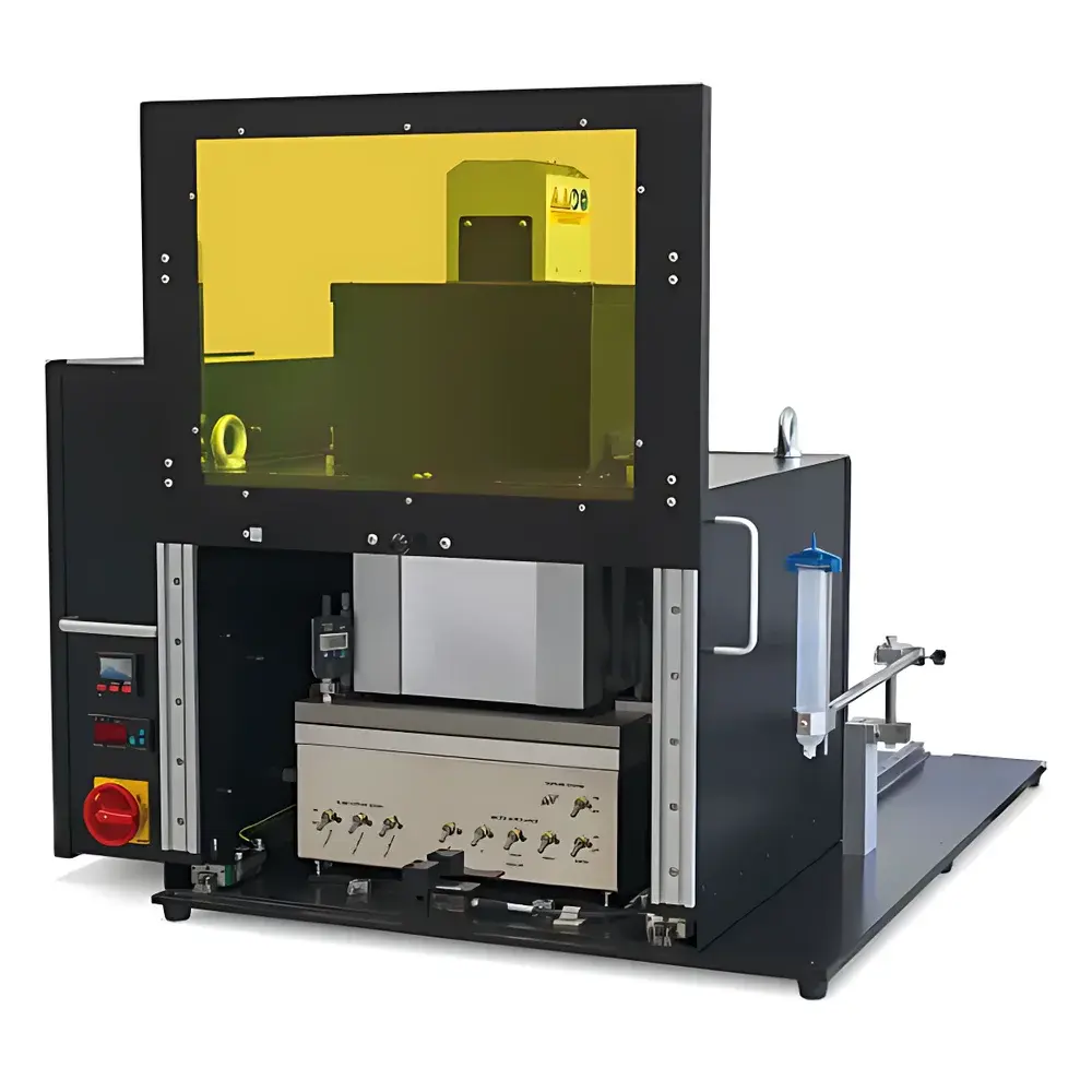
The SUSS UV-SFT Series Stamp-to-Substrate Alignment System is a compact, benchtop precision instrument engineered for the fabrication of high-fidelity working stamps used in micro- and nanoimprint lithography (NIL). Operating on the principle of contact-based optical alignment followed by UV-LED-driven polymerization, the UV-SFT enables deterministic, repeatable stamp-to-substrate registration under controlled mechanical force and thermal environment. Its core function is to establish sub-micron overlay accuracy between a master template (stamp) and a substrate coated with UV-curable resist—critical for replicating nanoscale features in R&D and high-volume manufacturing (HVM) environments. The system is purpose-built to complement SUSS’s MA/BA Gen4 8-inch mask aligner platform, forming an integrated process chain for mask-reticle metrology, stamp qualification, and imprint process development in advanced semiconductor packaging, MEMS/NEMS fabrication, micro-optics prototyping, and emerging AR/VR photonic sensor production.
Key Features
- Precision mechanical alignment stage with motorized X/Y/θ adjustment and real-time optical feedback for sub-500 nm overlay accuracy
- High-intensity UV-LED exposure module delivering ≥100 mW/cm² irradiance across 200 × 200 mm² or Ø200 mm area, with typ. illumination uniformity of ±2.5%
- Thermally stabilized chuck system supporting both ambient and elevated temperature processing (up to 120 °C), enabling compatibility with thermally sensitive resists and flexible substrates
- Modular vacuum and soft-contact clamping architecture for distortion-free handling of brittle wafers, thin glass, polymer films, and metal foils
- Field-upgradable design: supports retrofit from thermal-cure to UV-LED configuration without hardware replacement—preserving capital investment and extending system lifecycle
- Integrated force-sensing capability for programmable contact pressure control (0.1–5 N range), ensuring reproducible pattern transfer without stamp deformation
Sample Compatibility & Compliance
The UV-SFT accommodates a broad spectrum of substrate formats including rigid silicon, quartz, and sapphire wafers (2″ to 200 mm diameter), as well as square substrates up to 240 × 240 mm. It supports both hard stamps (e.g., fused silica, SiC, Ni) and compliant elastomeric molds (e.g., PDMS, fluorosilicone). All UV-curable chemistries—including acrylate-, epoxy-, and vinyl ether-based resists—are compatible, provided their absorption spectra overlap with the 365–405 nm emission band of the LED array. The system conforms to ISO 14644-1 Class 5 cleanroom operational guidelines and meets CE marking requirements for electromagnetic compatibility (EMC) and low-voltage directive compliance. For regulated environments, optional audit trail logging and user-access controls support adherence to FDA 21 CFR Part 11 and ISO 9001 quality management protocols.
Software & Data Management
Controlled via SUSS’s proprietary NanoAlign™ software suite, the UV-SFT provides intuitive workflow sequencing, parameter logging, and real-time alignment verification through live CCD imaging with 5×–50× digital zoom. All process recipes—including exposure dose (J/cm²), alignment offset vectors, contact force profiles, and temperature ramping schedules—are stored with timestamped metadata and version history. Export options include CSV, XML, and PDF reports compliant with internal QA documentation standards. Optional integration with factory MES systems is available via SECS/GEM protocol, enabling traceability from stamp fabrication to final device test.
Applications
- R&D-scale NIL stamp qualification and defect mapping prior to full-wafer imprint trials
- Production of replication masters for high-aspect-ratio photonic crystals and plasmonic metasurfaces
- Prototyping of microfluidic channel architectures with sub-100 nm feature fidelity
- Manufacturing of diffractive optical elements (DOEs) and microlens arrays for AR waveguides
- Low-damage patterning of organic semiconductors and perovskite thin films for flexible optoelectronics
- Process validation of hybrid bonding interfaces in 2.5D/3D IC packaging workflows
FAQ
What is the maximum allowable stamp thickness for UV-SFT operation?
Standard configurations support stamps up to 10 mm thick; custom chucks are available for thicker masters upon request.
Can the UV-SFT be integrated into an automated cluster tool environment?
Yes—equipped with front-end load port (FELP) interface and SECS/GEM communication, it supports integration into SMIF or FOUP-based automated fabs.
Does the system provide in-situ alignment verification before UV exposure?
Yes—dual-camera optical alignment with crosshair superposition and pixel-level offset calculation ensures <±0.3 µm pre-exposure registration confidence.
Is calibration traceable to national metrology institutes?
All alignment stages and UV intensity sensors are calibrated using NIST-traceable artifacts and documented per ISO/IEC 17025 procedures.
What maintenance intervals are recommended for the UV-LED module?
LED lifetime exceeds 20,000 hours at rated output; intensity recalibration is advised every 6 months or after 1,000 exposure cycles, whichever occurs first.


