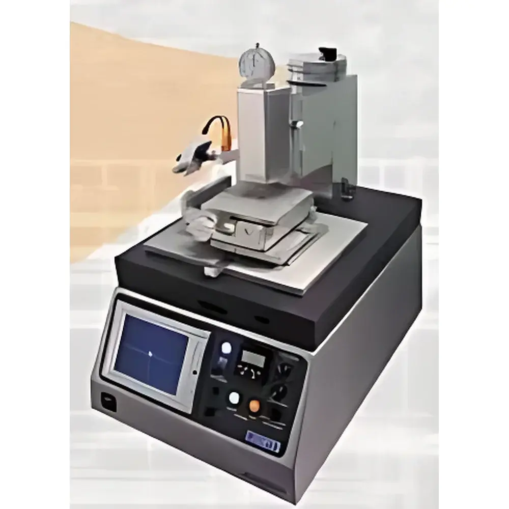
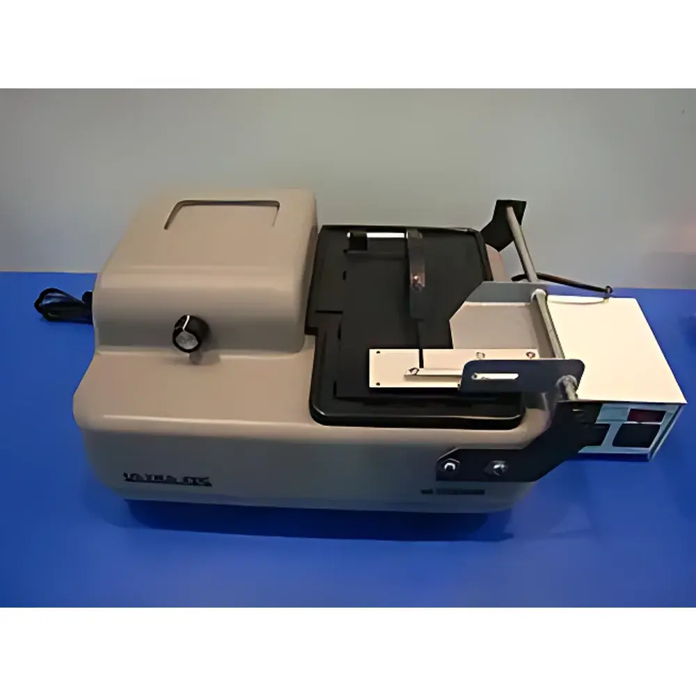
ULTRA TEC ASAP-1 Selective Area Precision Lapping & Polishing System
| Origin | USA |
|---|---|
| Manufacturer Type | Authorized Distributor |
| Origin Category | Imported |
| Model | ULTRA TEC ASAP-1 |
| Pricing | Available Upon Request |
Overview
The ULTRA TEC ASAP-1 Selective Area Precision Lapping & Polishing System is an engineered solution for controlled, repeatable cross-sectional sample preparation of advanced semiconductor packages and wafers. Based on precision mechanical lapping and sequential polishing principles—rather than thermal or chemical etching—the system enables deterministic material removal with sub-micron Z-axis positional control. It is specifically designed for failure analysis (FA), reliability testing, and quality assurance workflows in semiconductor laboratories where physical sectioning integrity directly impacts analytical validity in SEM, FIB-SEM, optical microscopy, and X-ray tomography. The ASAP-1 supports both front-side and back-side thinning of heterogeneous structures—including flip-chip interconnects, power devices, stacked die, BGA, PQFP, S-CSP, and MCM packages—without inducing delamination, cracking, or thermal artifact.
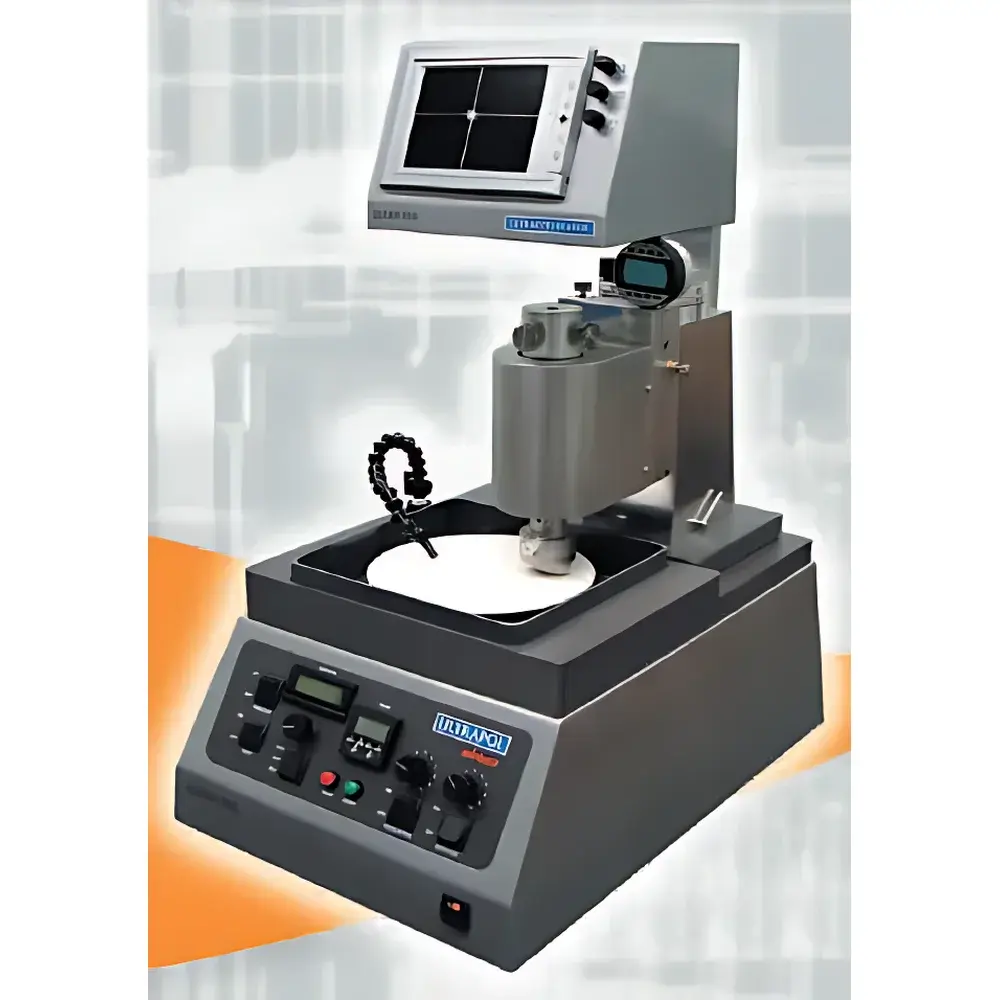
Key Features
- Z-axis positioning resolution down to 5 µm standard; optional 1 µm high-resolution encoder upgrade available for ultra-fine depth control.
- Integrated optical alignment station mounted above the work stage enables rapid, non-contact die-level targeting—eliminating iterative trial-and-error positioning common in legacy systems.
- Dual-mode operation: standard precision lapping mode for coarse-to-intermediate material removal, and optional ‘Power Polish’ mode for accelerated back-thinning of large-area flip chips or high-hardness substrates.
- Modular chuck system compatible with standard SEM stubs (e.g., 12.7 mm, 25.4 mm), wafer carriers (up to 200 mm), and custom fixtures for irregularly shaped dies and multi-chip modules.
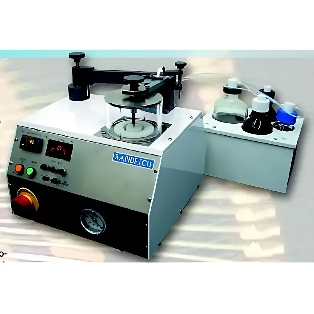
- Recirculating coolant/lubricant delivery with integrated filtration—supports reuse of diamond suspension slurries and water-based coolants while maintaining consistent thermal management and particle removal efficiency.
- Compact desktop footprint (W × D × H: 610 × 560 × 430 mm), low-noise brushless motor drive (<65 dB(A)), and ESD-safe enclosure compliant with ANSI/ESD S20.20.
Sample Compatibility & Compliance
The ASAP-1 accommodates a broad spectrum of package geometries and substrate materials, including silicon, SiC, GaN, ceramic substrates, molded epoxy, underfill polymers, and copper/tin-solder interconnects. It meets mechanical preparation requirements outlined in ASTM F2151 (Standard Guide for Failure Analysis of Integrated Circuits), JEDEC JEP122 (Failure Mechanisms and Models for Semiconductor Devices), and IPC-TM-650 2.1.1 (Cross-Sectioning of Printed Boards). All motion control firmware includes audit-trail logging capability aligned with GLP/GMP documentation practices. Optional configuration supports 21 CFR Part 11-compliant user authentication and electronic record retention when integrated with validated laboratory information management systems (LIMS).
Software & Data Management
The system operates via a dedicated embedded controller with touchscreen HMI interface—no external PC required. All process parameters (Z-depth target, feed rate, spindle RPM, coolant flow rate, dwell time) are stored as named protocols with versioned revision history. Protocol export/import is supported via USB 2.0 in CSV and XML formats for traceability and lab-wide method harmonization. Real-time position feedback and motor current monitoring provide diagnostic data for preventive maintenance scheduling. Optional Ethernet/IP connectivity enables remote monitoring and integration into centralized FA workflow orchestration platforms.
Applications
- Cross-sectional analysis of solder bump integrity, underfill voiding, and intermetallic compound (IMC) growth in flip-chip assemblies.
- Controlled back-grinding of power modules prior to TEM lamella extraction or EBIC imaging.
- Preparation of beveled edges for trench inspection in 3D NAND and DRAM stack characterization.
- Sectioning of heterogeneous integration structures (e.g., chiplets, fan-out wafer-level packaging) without interface delamination.
- Routine QC sectioning of PQFP, QFN, and BGA packages for lead-frame bondline verification and mold compound adhesion assessment.
- Wafer-level thinning for transmission-mode infrared (IR) inspection and photon emission microscopy (PEM).
FAQ
What package types are supported for mechanical decapsulation?
The ASAP-1 supports mechanical opening of S-CSP, BGA, flip-chip, power discrete devices, MCMs, and most plastic-encapsulated ICs without requiring acid fuming or plasma etching.
Is the system compatible with automated SEM stage navigation?
Yes—coordinate output (X/Y/Z in µm) can be exported in ASCII format and aligned with SEM stage coordinates using third-party registration software for post-polish imaging correlation.
Can the same setup be used for both lapping and final polishing steps?
Yes—the modular abrasive wheel and polishing pad mounting system allows tool-free switching between 15 µm diamond lapping wheels and 0.05 µm colloidal silica polishing cloths.
Does the system require compressed air or external chillers?
No—coolant recirculation is self-contained; only standard 110–240 VAC power and tap-water supply for initial fill are required.
What maintenance intervals are recommended?
Daily coolant level check and filter cleaning; quarterly calibration of Z-axis encoder and annual bearing inspection per manufacturer’s service manual.


