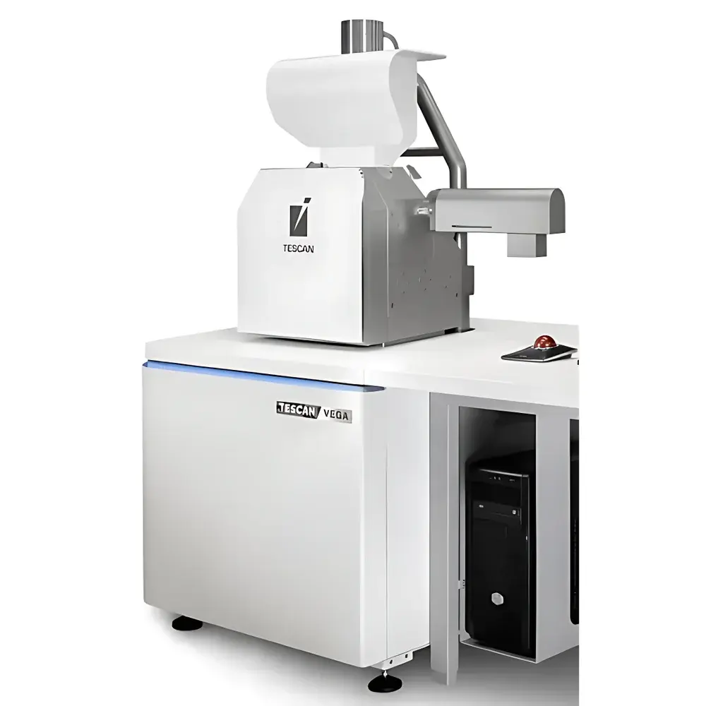
TESCAN VEGA Scanning Electron Microscope (SEM)
| Brand | TESCAN |
|---|---|
| Origin | Czech Republic |
| Model | TESCAN VEGA |
| Instrument Type | Floor-standing Conventional SEM |
| Electron Source | Tungsten Filament |
| Secondary Electron Resolution | 3.0 nm @ 30 kV |
| Magnification Range | 2× – 1,000,000× |
| Accelerating Voltage | 200 V – 30 kV (continuously adjustable) |
| Backscattered Electron Resolution | 3.5 nm @ 30 kV |
Overview
The TESCAN VEGA Scanning Electron Microscope (SEM) is a fourth-generation tungsten-filament SEM engineered for high-resolution surface imaging and integrated microanalysis in routine laboratory environments. Operating on the principle of raster-scanned electron beam interaction with solid specimens, the VEGA generates topographic, compositional, and crystallographic contrast signals—including secondary electrons (SE), backscattered electrons (BSE), and characteristic X-rays—enabling nanoscale morphological characterization down to 3.0 nm resolution at 30 kV. Designed for robustness, operational simplicity, and analytical versatility, the VEGA platform serves as a foundational tool in materials science, life sciences, geosciences, and industrial quality assurance laboratories where reproducible, high-fidelity imaging and elemental mapping are required without the complexity or cost of field-emission systems.
Key Features
- Integrated Essence™ Software Platform: Unifies real-time SEM imaging and energy-dispersive X-ray spectroscopy (EDS) analysis within a single graphical interface—eliminating workflow fragmentation between acquisition and quantification.
- In-Flight Beam Tracing™ Technology: Replaces conventional mechanical apertures with dynamic, software-controlled beam alignment; enables rapid optimization of probe current, spot size, and signal-to-noise ratio without manual intervention.
- Wide Field Optics™: Delivers seamless magnification from 2× to 1,000,000× using a single optical path—removing dependency on auxiliary optical navigation cameras while maintaining geometric fidelity across low- and high-magnification regimes.
- SingleVac™ Mode: Standard variable-pressure capability permits direct observation of non-conductive, hydrated, or beam-sensitive specimens (e.g., polymers, biological tissues, ceramics) without metal coating or cryo-preparation.
- 3D Beam Technology™: Supports stereo-pair acquisition and real-time anaglyph rendering for depth perception—enhancing defect localization, fracture surface analysis, and dimensional metrology workflows.
- Essence™ 3D Collision Avoidance: Visualizes real-time spatial relationships among stage position, detector geometry, and chamber fixtures—preventing mechanical interference during automated multi-location acquisitions or tilt-series experiments.
- Vacuum Buffering Unit: Reduces mechanical pump runtime by up to 70% through intelligent pressure staging—lowering acoustic noise, power consumption, and maintenance frequency while extending pump service intervals.
- Modular Detector Architecture: Supports factory-integrated or field-upgradable detectors including YAG-based cathodoluminescence (CL), cooled BSE, and fiber-coupled Raman spectrometers—enabling correlative SEM-Raman or SEM-CL structural studies.
Sample Compatibility & Compliance
The VEGA accommodates specimens up to 200 mm in diameter and 100 mm in height under standard configuration. Its SingleVac™ mode supports pressures up to 130 Pa, enabling stable imaging of insulating powders, uncoated biological sections, and porous geological samples. The system complies with IEC 61000-6-3 (EMC emission standards) and IEC 61000-6-2 (immunity), and meets CE marking requirements for laboratory instrumentation. For regulated environments, optional audit-trail logging, user access control, and electronic signature modules align with FDA 21 CFR Part 11 and EU Annex 11 expectations when deployed in GLP/GMP-compliant QA/QC labs.
Software & Data Management
Essence™ provides a unified, scriptable environment supporting ASTM E1558–22 (standard guide for SEM image acquisition), ISO 16700 (quantitative EDS microanalysis), and USP (analytical instrument qualification). All acquisitions include embedded metadata (kV, WD, dwell time, aperture setting, detector type), and raw data is stored in vendor-neutral TIFF/JSON bundles compatible with third-party analysis suites (e.g., ImageJ, DTSA-II, HyperSpy). Batch processing, template-driven acquisition, and remote monitoring via secure HTTPS are supported—facilitating integration into LIMS and enterprise data management systems.
Applications
- Materials Science: Fractography of metallic alloys, dispersion analysis of polymer composites, interfacial characterization in cementitious matrices, fiber morphology in textiles and paper.
- Life Sciences: Cellular ultrastructure imaging in fixed tissue, particle uptake studies in drug delivery carriers, pollen grain topography, biofilm architecture on medical implants.
- Geosciences: Mineral phase identification via BSE-Z contrast, porosity quantification in reservoir rocks, microfossil preservation assessment, slag inclusion analysis in metallurgical byproducts.
- Industrial QA/QC: Coating thickness verification, solder joint integrity inspection, contaminant identification in semiconductor packaging, wear debris morphology in lubricants.
FAQ
Is the TESCAN VEGA suitable for uncoated biological samples?
Yes—SingleVac™ mode allows imaging of hydrated or non-conductive biological specimens at pressures up to 130 Pa without sputter coating.
What vacuum level is required for EDS analysis?
EDS acquisition requires high vacuum (≤1 × 10⁻³ Pa); the system automatically transitions between SingleVac™ and high-vacuum modes based on detector selection.
Can the VEGA be upgraded with a field-emission gun?
No—the VEGA platform is optimized for tungsten-filament performance and thermal stability; TESCAN offers FE-SEM alternatives (e.g., MIRA series) for sub-nanometer resolution requirements.
Does Essence™ support automated particle analysis?
Yes—via optional ParticleMetric™ module, which enables threshold-based segmentation, size distribution histograms, and shape factor classification per ISO 13322-1.
What is the typical service interval for the tungsten filament?
Under standard operating conditions (20 kV, 1 nA probe current), filament lifetime averages 150–200 hours; replacement is user-performed in <15 minutes without venting the column.


