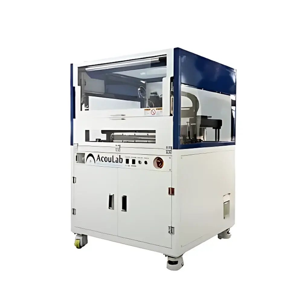
Acoulab SAM-DENEB Scanning Acoustic Microscope (SAM)
| Brand | Acoulab |
|---|---|
| Origin | South Korea |
| Model | SAM-DENEB |
| Instrument Type | Digital Scanning Acoustic Microscope |
| Scan Range (X-Y) | 350 mm × 350 mm |
| Spatial Resolution (X-Y) | 0.5 µm |
| Ultrasonic Transducer Frequency Range | 1–500 MHz |
| A/D Sampling Rate | 2 GHz |
| Analog Bandwidth | 1 GHz |
| X-Y Scan Speed | 1000 mm/s |
| X-Y Repeatability | ±0.5 µm |
| Z-Axis Scan Range | 70 mm |
| Z-Axis Resolution | 2.5 µm |
Overview
The Acoulab SAM-DENEB Scanning Acoustic Microscope is a high-precision, non-destructive evaluation (NDE) instrument engineered for subsurface defect characterization in microelectronic packages, advanced power modules, and heterogeneous material systems. It operates on the principle of pulse-echo ultrasonic imaging—transmitting high-frequency acoustic waves (1–500 MHz) into a sample immersed in coupling fluid (typically deionized water), then detecting time-resolved reflections from acoustic impedance mismatches at internal interfaces. These echoes are digitized at 2 GHz sampling rate with 1 GHz analog bandwidth, enabling nanosecond-scale temporal resolution and sub-micron spatial localization. Unlike optical or electron microscopy, SAM provides depth-resolved, volumetric contrast without sample sectioning, making it indispensable for failure analysis labs, semiconductor quality assurance teams, and materials R&D centers requiring traceable, repeatable internal inspection under GLP-compliant workflows.
Key Features
- High-fidelity acoustic imaging with 0.5 µm lateral resolution and 2.5 µm axial (Z) resolution across a 350 mm × 350 mm scanning envelope—optimized for full-package inspection of large-format IGBT modules, ceramic substrates, and multi-layer PCBs.
- Dual-axis linear servo motor stage delivering 1000 mm/s scan velocity and ±0.5 µm positional repeatability—ensuring throughput without compromising measurement fidelity.
- Multi-mode scanning architecture supporting A-scan (time-domain waveform), B-scan (cross-sectional slice), C-scan (planar projection at fixed depth), X-scan (multi-depth layer stacking), and volumetric 3D reconstruction via sequential C-scan acquisition.
- Low-noise RF front-end and calibrated transducer array enabling quantitative amplitude and time-of-flight analysis—critical for distinguishing voids (<5 µm diameter), delaminations (<100 nm thickness), and particulate inclusions in encapsulated die attach layers.
- Integrated acoustic impedance calibration routines compliant with ASTM E1158 and ISO 16810 standards for NDT equipment validation—supporting audit-ready documentation for ISO 9001, IATF 16949, and AEC-Q200 qualification processes.
Sample Compatibility & Compliance
The SAM-DENEB accommodates a broad range of electrically insulated, acoustically transmissive samples—including molded IC packages (Flip Chip, BGA, FBGA, QFN), discrete power devices (IGBTs, SiC MOSFETs), multilayer ceramic capacitors (MLCCs), sputtering targets (ITO, Mo, Cu), wafer-level interposers, and structural components (engine pistons, weld zones, composite laminates). Samples up to 350 mm × 350 mm footprint and 70 mm height can be accommodated without disassembly. All operational modes comply with IEC 61000-6-3 (EMC emissions) and IEC 61000-6-2 (immunity), while acoustic exposure levels remain well below ICNIRP occupational safety thresholds—no radiation hazard or ionizing energy involved. Data acquisition workflows support FDA 21 CFR Part 11–compliant electronic signatures and audit trails when integrated with validated LIMS or ELN platforms.
Software & Data Management
The proprietary Acoulab SAM Studio v5.x software provides real-time image rendering, automated defect segmentation (threshold-based + machine learning-assisted classification), and metrology tools for void area quantification, delamination length mapping, and depth-profiled acoustic attenuation calculation. Raw RF data (I/Q format) is stored in HDF5 containers with embedded metadata (transducer ID, gain settings, temperature, operator ID, timestamp), ensuring FAIR (Findable, Accessible, Interoperable, Reusable) data principles. Export options include TIFF (8/16-bit), CSV (coordinate + amplitude), STL (3D surface mesh), and DICOM-SAM extensions for integration into enterprise PACS environments. Software validation documentation (IQ/OQ/PQ protocols) and change control logs are provided per GMP Annex 11 requirements.
Applications
- Semiconductor Packaging: Detection of die attach voids (>3 µm), mold compound delamination at chip-to-substrate interfaces, wire bond lift-off, and underfill cracking in advanced fan-out wafer-level packages (FO-WLP).
- Power Electronics: Integrity assessment of solder joints and direct bonded copper (DBC) layers in IGBT modules; thermal interface material (TIM) coverage uniformity mapping in EV traction inverters.
- Passive Components: Volumetric inspection of MLCC electrode misalignment, internal porosity in high-K dielectrics, and termination delamination in automotive-grade capacitors.
- Advanced Materials: Characterization of porosity distribution in additively manufactured metal parts, fiber-matrix debonding in carbon-fiber composites, and inclusion clustering in sputter targets used for display manufacturing.
- Industrial QA: In-process weld integrity verification (e.g., aluminum laser welds in battery enclosures), casting porosity screening in aerospace turbine blades, and coating adhesion testing on thermal barrier coatings.
FAQ
What types of defects can the SAM-DENEB detect in semiconductor packages?
It detects subsurface discontinuities including voids, delaminations, cracks, particle inclusions, and bonding failures—down to ~3 µm lateral size and <100 nm interfacial gap height—without physical sectioning.
Is water immersion mandatory during scanning?
Yes—deionized water serves as an acoustic coupling medium to transmit ultrasound efficiently into solid samples; alternative couplants (e.g., glycerol) may be used for temperature-sensitive or hydrophobic materials.
Can the system perform automated pass/fail analysis for production line use?
Yes—via customizable rule-based inspection scripts that trigger alerts based on user-defined thresholds for void area %, delamination length, or echo amplitude deviation from reference standards.
Does the SAM-DENEB support 3D volume reconstruction and export?
Yes—sequential C-scan acquisition across Z-depth enables isotropic voxel reconstruction (0.5 µm × 0.5 µm × 2.5 µm); volumes can be exported as STL, OBJ, or segmented label maps for CAD overlay or finite element modeling.
How is measurement traceability ensured for ISO/IEC 17025 accreditation?
Through documented transducer calibration certificates (NIST-traceable reference blocks), stage positioning verification reports (laser interferometer validated), and software version-controlled audit logs meeting ILAC-G8:2023 requirements.


