Fastmicro FM-PS-PRS-V01 Wafer Surface Particle Inspection System
| Brand | Fastmicro |
|---|---|
| Country of Origin | Netherlands |
| Model | FM-PS-PRS-V01 |
| Detection Principle | Mie Scattering |
| Minimum Detectable Particle Size | 0.5 µm (PSL) |
| Measurement Speed | Full-surface imaging in seconds |
| Position Accuracy | 80 µm |
| Position Repeatability | 30 µm |
| Size Accuracy (PSL) | <20% error |
| Surface Roughness Requirement | Ra < 50 nm |
| Output Formats | KLARF, Excel |
| Interface | USB, Ethernet |
| Contactless Operation | Yes |
| Compliance | Designed for ISO 14644-1 cleanroom environments and SEMI S2/S8 safety standards |
Overview
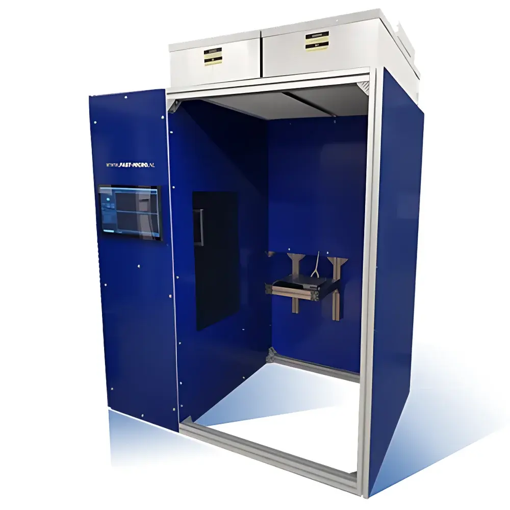
The Fastmicro FM-PS-PRS-V01 Wafer Surface Particle Inspection System is a high-precision, non-contact optical metrology instrument engineered specifically for contamination control in semiconductor front-end manufacturing and flat-panel display (FPD) production. It operates on the physical principle of Mie scattering — where monochromatic, collimated illumination interacts with submicron-scale particulate contaminants on ultra-smooth surfaces, generating angularly resolved scattering signatures that are captured by a calibrated CMOS imaging sensor. Unlike traditional dark-field or laser scanning systems constrained by fixed field-of-view or mechanical raster limitations, the FM-PS-PRS-V01 employs a modular, scalable optical architecture enabling seamless inspection of wafers up to 300 mm diameter — or arbitrarily large substrates such as Gen 10.5 glass panels — without stitching artifacts or positional drift. Its core function is quantitative particle counting, spatial mapping, and size classification of surface-bound contaminants ≥0.5 µm (polystyrene latex, PSL), supporting critical process verification steps including post-CMP residue assessment, pre-lithography mask inspection, and post-clean validation.
Key Features
- Patented Mie scattering detection engine optimized for low-roughness (<50 nm Ra) dielectric and silicon surfaces
- Sub-second full-field imaging capability across configurable scan areas — no mechanical stage movement required for standard wafer formats
- Real-time particle localization with positional accuracy of ±80 µm and repeatability of ±30 µm
- Size classification accuracy <20% deviation for PSL standards ≥500 nm; validated per ISO 21507:2019 for particle sizing instruments
- Fully contactless operation — zero risk of surface scratching, electrostatic discharge, or cross-contamination
- Modular hardware design supports integration into automated load-port interfaces (SECS/GEM compliant) and factory host systems
- Onboard calibration routines traceable to NIST-traceable PSL reference materials
Sample Compatibility & Compliance
The FM-PS-PRS-V01 accommodates bare silicon wafers (200 mm / 300 mm), photomasks (quartz/chrome), low-k dielectrics, and TFT-LCD glass substrates (up to 3370 × 2940 mm). Surface topography requirements are strictly defined: arithmetic average roughness (Ra) must remain below 50 nm to ensure scattering signal fidelity and minimize false positives from intrinsic surface texture. The system conforms to SEMI F47-0220 (electrical safety), SEMI S2-0220 (health and safety), and ISO 14644-1 Class 1–5 cleanroom compatibility. All firmware and data handling protocols support audit-ready operation under ISO 9001, IATF 16949, and semiconductor-specific quality frameworks requiring full traceability.
Software & Data Management
The embedded inspection software provides real-time visualization of particle maps overlaid on high-resolution substrate thumbnails, with configurable thresholds for size binning (e.g., 0.5–1.0 µm, 1.0–5.0 µm, >5.0 µm). Quantitative outputs include total particle count per zone, spatial density distribution (particles/cm²), centroid coordinates (X/Y in mm), equivalent spherical diameter (ESD), and annotated TIFF/PNG images with particle ID tagging. Export formats comply with industry-standard defect data interchange protocols: KLARF 2.0/3.0 for integration with yield management systems (YMS) such as Applied Materials Discover or KLA ICOS, plus CSV/Excel for statistical process control (SPC) analysis. Data transmission occurs via Gigabit Ethernet or USB 3.2 Gen 2, with optional TLS 1.2 encryption and user-role-based access control aligned with FDA 21 CFR Part 11 requirements for electronic records and signatures.
Applications
- Post-chemical-mechanical polishing (CMP) particle residue verification on logic and memory wafers
- Photomask and reticle surface cleanliness screening prior to lithography exposure
- In-line monitoring of wet bench cleaning efficiency (SC1, SC2, DHF) across multiple process lots
- Defect root-cause analysis during advanced packaging processes involving bumping, RDL, or TSV formation
- Qualification of EUV pellicle integrity and contamination accumulation over time
- Flat-panel display manufacturing: particle inspection on color filter arrays, touch sensor layers, and OLED encapsulation substrates
FAQ
What particle sizes can the FM-PS-PRS-V01 reliably detect?
It detects polystyrene latex (PSL) particles ≥0.5 µm with statistically significant signal-to-noise ratio; optimal sizing accuracy applies to particles ≥500 nm per ISO 21507.
Does the system require vacuum or inert gas environments?
No — it operates under ambient cleanroom conditions (Class 1–5); no vacuum chamber or purge gas interface is needed.
Can it inspect patterned wafers or only bare surfaces?
It is validated for both bare silicon and patterned wafers with feature pitches >1 µm; dense sub-100 nm patterns may require application-specific sensitivity tuning.
Is KLARF export compatible with KLA, Applied Materials, or Hermes YMS platforms?
Yes — KLARF 2.0 and 3.0 exports are fully interoperable with major yield management ecosystems and have been verified in production fabs worldwide.
How is measurement repeatability ensured across different operators or shifts?
Built-in daily self-calibration using integrated PSL reference targets, combined with operator-independent SOP-driven workflows and electronic audit trails, ensures Gage R&R <10% per AIAG MSA guidelines.


