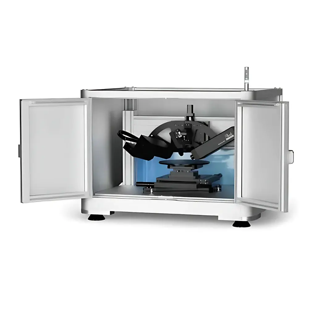
Accurion RSE Referenced Spectroscopic Ellipsometer for Rapid Thin-Film and Surface Characterization
| Brand | Accurion |
|---|---|
| Origin | Switzerland |
| Model | RSE Referenced Spectroscopic Ellipsometry Fast Inspection System |
| Spectral Range | 450–900 nm |
| Spot Size | 50 × 100 µm (at 60° incidence) |
| Thickness Measurement Range | <1 nm to 10 µm |
| Acquisition Rate | 200 full spectroscopic ellipsometric spectra per second |
| Mapping Area | 100 mm × 100 mm in ≤12 min |
| Data Processing | Real-time look-up table (LUT)-based fitting |
| Compliance | Designed for ISO/IEC 17025-aligned QC environments, supports GLP/GMP traceability via audit-ready software logs |
Overview
The Accurion RSE Referenced Spectroscopic Ellipsometer is an engineered solution for high-throughput, non-contact optical characterization of thin films and surface layers in industrial quality control and R&D laboratories. Unlike conventional rotating-element or phase-modulated ellipsometers, the RSE operates on a referenced differential measurement principle: it simultaneously illuminates both a stable reference sample and the target specimen under identical optical conditions, detecting only the relative change in polarization state between them. This architecture eliminates moving parts—no rotating compensators, no photoelastic modulators—and inherently suppresses common-mode noise from source drift, thermal fluctuations, and environmental vibration. The system acquires full spectroscopic ellipsometric data (Ψ and Δ across 450–900 nm) at up to 200 Hz, enabling sub-second spectral snapshots with intrinsic wavelength calibration stability. Its core application domain includes real-time thickness mapping of dielectric, semiconductor, and organic thin films on transparent or reflective substrates—particularly where nanoscale resolution (<1 nm), process repeatability, and integration into inline or semi-automated workflows are critical.
Key Features
- Differential referencing architecture ensures long-term measurement stability without recalibration between runs
- Fixed-optics design with no mechanical modulation components—maximizes reliability and minimizes maintenance
- High-speed spectral acquisition: 200 complete Ψ(λ)/Δ(λ) spectra per second over 450–900 nm
- Micro-spot capability: 50 × 100 µm elliptical probe beam at 60° angle of incidence, optimized for localized analysis and edge detection
- Real-time data reduction via precomputed look-up tables (LUTs), enabling immediate thickness and refractive index output during acquisition
- Integrated motorized X/Y stage with sub-micron positioning repeatability for automated wafer-scale mapping (e.g., 100 mm × 100 mm in ≤12 minutes)
- Modular optical head design compatible with vacuum chambers, gloveboxes, or ambient cleanroom integration
Sample Compatibility & Compliance
The RSE accommodates rigid and flat substrates including silicon wafers, fused silica, sapphire, glass, and metal-coated plates. It supports transparent, semi-transparent, and opaque base materials—provided the film stack exhibits measurable polarization contrast in the visible-NIR range. No conductive coating or vacuum requirement is necessary. The system complies with metrological best practices for optical thin-film metrology: all measurements are traceable to NIST-calibrated spectral radiance standards; raw data files retain full spectral metadata (wavelength grid, incidence angle, polarization state, detector gain settings). Software export formats include ASTM E2838-compliant .csv and ISO 14644-1-aligned reporting templates. For regulated environments, optional audit trail logging meets FDA 21 CFR Part 11 requirements when deployed with validated IT infrastructure.
Software & Data Management
Accurion’s proprietary RSE Control Suite provides instrument control, real-time visualization, model-based fitting, and statistical mapping. The software implements a two-stage fitting workflow: first, users define a physically realistic optical model (layer stack, dispersion relations, interface roughness); second, the system generates a high-resolution LUT covering expected parameter ranges (e.g., n/k dispersion, thickness, surface roughness). During acquisition, each spectrum is matched against the LUT in <50 ms, delivering thickness and optical constants with uncertainty estimates derived from spectral residual analysis. All raw interferograms, fitted parameters, confidence intervals, and model definitions are stored in HDF5 format with embedded provenance tags (operator ID, timestamp, environmental sensor readings). Batch processing supports SPC charting, Cp/Cpk calculation, and export to MES or SAP QM modules via REST API.
Applications
- Process monitoring of ALD, PECVD, and spin-coated dielectric films on 200 mm and 300 mm wafers
- Thickness uniformity assessment of anti-reflective coatings, ITO layers, and barrier films on display glass
- Quantitative analysis of native oxide growth, contamination layers, and interfacial diffusion in semiconductor packaging
- In-line verification of monolayer and sub-nanometer organic films (e.g., SAMs, graphene oxide) on functionalized surfaces
- Research-grade characterization of perovskite photovoltaic stacks, MOF thin films, and bio-functionalized sensor surfaces
- Failure analysis of delamination, blistering, and interfacial void formation through depth-resolved optical modeling
FAQ
Does the RSE require periodic recalibration using standard reference samples?
No—its referenced differential architecture inherently corrects for source intensity drift and detector responsivity changes. A single baseline reference measurement suffices for extended operation (typically >8 hours under stable lab conditions).
Can the RSE measure multilayer stacks with buried interfaces?
Yes, provided the optical contrast between adjacent layers is sufficient within the 450–900 nm band and the total stack thickness remains within the coherence length of the light source (~10 µm). Modeling requires appropriate dispersion models (e.g., Tauc-Lorentz, Cody-Lorentz) for each layer.
Is vacuum or inert atmosphere operation supported?
The optical head is modular and can be mounted on vacuum flanges (CF-63 or KF-40). Optional purge ports allow nitrogen or argon purging for moisture-sensitive samples.
What level of training is required for routine QC operation?
Operators require ≤4 hours of hands-on instruction to perform wafer mapping, thickness reporting, and basic model adjustment. Advanced optical modeling and LUT generation are typically performed by metrology engineers.
How does the RSE handle rough or patterned surfaces?
Surface roughness is modeled as an effective medium layer (Bruggeman approximation). For patterned structures (e.g., gratings), the system reports average film properties over the 50 × 100 µm spot; higher spatial resolution requires optional micro-spot upgrade or complementary AFM correlation.


