4D TECHNOLOGY 280SI Four-Point Probe Sheet Resistance and Resistivity Tester
| Brand | 4D TECHNOLOGY |
|---|---|
| Origin | USA |
| Model | 280SI |
| Automation Level | Fully Automatic |
| Sheet Resistance Range | 0.001 Ω/□ to 8×10⁵ Ω/□ (Standard) |
| Sheet Resistance Accuracy | <0.1% |
| Resistivity Range | 0.001 Ω·cm to 8×10⁵ Ω·cm (derived from sheet resistance and user-input film thickness) |
| Resistivity Accuracy | <0.1% |
| Substrate Size Support | 2–8 inch wafers (333-series supports up to 12 inch |
| Test Current Accuracy | <0.1% |
| Probe Force Adjustment Range | 90–200 g |
| Probe Tip Material | Tungsten carbide with sapphire bushings |
| Edge Correction Capability | Yes, within 3 mm from wafer edge |
| Measurement Speed | >45 points/min |
| Repeatability | <0.2% (per substrate) |
| Data Output | 2D/3D contour maps, statistical summaries, Excel-compatible reports |
Overview
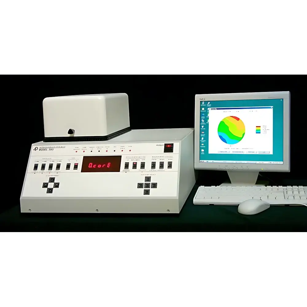
The 4D TECHNOLOGY 280SI Four-Point Probe Sheet Resistance and Resistivity Tester is a precision metrology instrument engineered for quantitative electrical characterization of conductive and semiconductive thin films in semiconductor fabrication, display manufacturing, photovoltaics, and advanced materials R&D. Based on the established four-point collinear probe method—compliant with ASTM F84 and ISO 10700—the system eliminates contact resistance errors by separating current injection and voltage sensing functions across four independent, mechanically stable probes. The 280SI employs a high-stability constant-current source and low-noise nanovolt measurement circuitry to deliver traceable, repeatable sheet resistance (Rs) values across an exceptionally wide dynamic range—from 1 mΩ/□ to 800 kΩ/□ in standard configuration—with optional extensions down to 0.1 mΩ/□ and up to 8 GΩ/□ or 800 GΩ/□ depending on probe geometry and material-specific calibration. Resistivity (ρ) is computed in real time using the relation ρ = Rs × t, where film thickness (t) is entered by the operator or imported via external database integration. All measurements are referenced to NIST-traceable standards and support GLP/GMP-compliant audit trails when configured with FDA 21 CFR Part 11–enabled software.
Key Features
- Fully automated motorized X-Y-Z stage with programmable point mapping—supports arbitrary grid patterns, radial scans, or custom coordinate lists for spatial uniformity analysis
- Adjustable probe force (90–200 g) with tungsten carbide tips and sapphire bushings ensuring long-term inter-probe spacing stability (>250,000 actuations per probe set, per manufacturer specification)
- Edge correction algorithm enabling valid Rs measurements within 3 mm of substrate perimeter—critical for process monitoring on full-wafer lots
- Modular probe interchangeability: supports A-, B-, K-, M-, and N-type probes per ASTM F1529; MR-type probes available for ultra-thin films (<3 nm, e.g., 30 Å), minimizing current spreading artifacts
- Standalone operation mode: onboard display and keypad allow single-point Rs acquisition without PC connection—ideal for rapid inline verification or irregular sample geometries
- Real-time data visualization: 2D heatmaps, 3D topographic resistivity surfaces, and statistical overlays (mean, σ, min/max, histogram) generated during acquisition
Sample Compatibility & Compliance
The 280SI accommodates rigid planar substrates including silicon, GaAs, SiC, sapphire, glass, and flexible metal foils. Standard configurations support 2–8 inch circular wafers; optional 333-series stages extend capability to 12 inch wafers, while the 1100-series platform handles large-area flat panels up to 2160 mm × 2400 mm—common in Gen 8.5+ TFT-LCD and thin-film PV production. Square samples up to 156 mm × 156 mm are also supported. All mechanical and electrical designs conform to IEC 61000-6-2 (immunity) and IEC 61000-6-3 (emission) standards. Measurement methodology adheres to ASTM F84 (standard test method for sheet resistance of semiconductor wafers using four-point probes), ASTM F1529 (classification of probe types), and ISO 10700 (resistivity measurement of thin conductive films). Optional temperature-controlled chucks (−40 °C to +150 °C) enable thermal coefficient of resistance (TCR) profiling under controlled ambient conditions.
Software & Data Management
The 280SI operates with 4D’s proprietary WinProbe™ software suite, compatible with Windows 10/11 (64-bit). The interface supports script-driven measurement sequences, multi-user role-based access control, and full electronic record retention—including timestamped raw voltage/current readings, probe position logs, environmental metadata (ambient T/RH), and operator ID. Audit trail functionality meets FDA 21 CFR Part 11 requirements for regulated environments, with digital signature enforcement and immutable log archiving. Data export options include CSV, XML, and native Excel (.xlsx) formats with embedded formulas for derived parameters (e.g., dopant concentration estimation via mobility assumptions). Integration with MES/SPC systems is enabled via TCP/IP, Modbus TCP, and OPC UA protocols; optional RESTful API allows direct ingestion into Python- or LabVIEW-based analytics pipelines.
Applications
- Semiconductor front-end process control: monitoring ion implant dose uniformity, diffusion junction depth, and post-anneal sheet resistance stability in CMOS, RF, and power device fabs
- Flat panel display manufacturing: characterizing ITO, AZO, and metal mesh electrodes on Gen 6–Gen 10 glass substrates for OLED and LCD lines
- Photovoltaic R&D and production: quantifying emitter sheet resistance in PERC, TOPCon, and heterojunction solar cells; evaluating transparent conductive oxide (TCO) layers on CIGS and CdTe modules
- Advanced packaging: mapping Rs across redistribution layers (RDLs), copper pillars, and embedded die substrates in fan-out wafer-level packaging (FOWLP)
- Academic and national lab research: correlating doping profiles with Hall effect data, validating ALD/CVD film growth models, and benchmarking novel 2D materials (graphene, MoS₂, MXenes)
FAQ
Does the 280SI require external calibration standards?
No—each system ships with a certified NIST-traceable calibration resistor array and built-in self-test routines. Annual verification against primary standards is recommended but not mandatory for non-regulated use.
Can the 280SI measure non-uniform or patterned wafers?
Yes—programmable point selection allows targeted measurement on active die areas, scribe lanes, or test structures without interference from metallization or isolation trenches.
Is film thickness input mandatory for resistivity calculation?
Yes—resistivity derivation requires user-supplied or externally linked thickness data. The system does not perform ellipsometry or profilometry; it assumes thickness is known from complementary metrology.
What probe type is recommended for measuring doped silicon epitaxial layers?
B-type probes (25 µm tip radius, 1.0 mm probe spacing) are optimal for standard Si wafers; for ultra-shallow junctions (<100 nm), K-type probes (12.5 µm radius, 0.5 mm spacing) minimize lateral current spread error.
How is data integrity ensured during high-throughput production runs?
All measurements are time-stamped, digitally signed, and written to redundant storage (local SSD + network share). Failed acquisitions trigger automatic retest logic and flag outliers using modified Thompson τ criterion.


