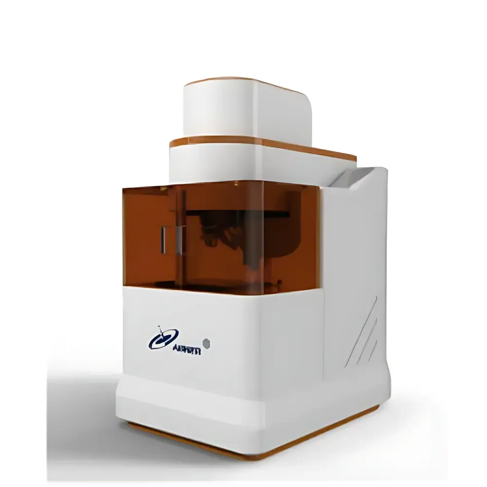
Abner ABN-MLM-001 Maskless Direct-Write Lithography System
| Brand | Abner |
|---|---|
| Origin | Jiangsu, China |
| Model | ABN-MLM-001 |
| Resolution | 0.3 µm |
| Light Source Wavelength | 405 nm |
| Maximum Optical Power | 300 mW |
| Alignment Accuracy (Frontside) | ±0.1 µm (within 1 mm) |
| Alignment Accuracy (Backside) | ±1 µm (within 2.5 mm) |
| Writing Speed | 3–150 mm²/min |
| Substrate Compatibility | 2″–8″ wafers, glass, flexible substrates |
Overview
The Abner ABN-MLM-001 Maskless Direct-Write Lithography System is a precision micro/nano-fabrication instrument engineered for digital photolithography without physical photomasks. It employs a high-speed Digital Micromirror Device (DMD) to dynamically modulate UV light at 405 nm, enabling pixel-level control over exposure patterns directly onto photoresist-coated substrates. Unlike conventional projection or contact lithography systems, this platform eliminates the need for mask fabrication, mask alignment, and mask storage—reducing both time-to-pattern and non-recurring engineering (NRE) costs. The system operates on the principle of vector-scan or raster-scan pattern generation, where CAD or GDSII layout data is converted in real time into spatially resolved illumination, allowing sub-micron feature definition with high positional fidelity. Designed for research-grade process development, it supports iterative prototyping under cleanroom-compatible environmental conditions and integrates seamlessly into academic, R&D, and pilot-line semiconductor workflows.
Key Features
- DMD-based digital light modulation for true maskless exposure—enabling instant pattern updates without mechanical mask handling or re-alignment.
- Native support for industry-standard layout formats including GDSII and DXF, with built-in pattern editing, layer management, and Boolean operations.
- High-precision XYZθ motorized stage with closed-loop encoders ensures repeatable positioning and multi-layer overlay alignment (frontside alignment accuracy: ±0.1 µm within 1 mm).
- UV optical engine optimized for 405 nm wavelength, delivering up to 300 mW output power with uniform intensity distribution across the exposure field.
- Programmable dose control via shutter timing and DMD duty cycle modulation—supporting grayscale lithography and variable-threshold exposure for 3D resist profiling.
- Modular substrate holder accommodating 2″–8″ wafers, fused silica, quartz, glass slides, and polymer-based flexible substrates.
- Integrated safety architecture compliant with IEC 60825-1 (Class 3B laser safety), featuring interlocked enclosure doors, beam shutter fail-safes, and real-time power monitoring with audible/visual alarms.
Sample Compatibility & Compliance
The ABN-MLM-001 is validated for use with standard positive and negative photoresists (e.g., AZ series, SU-8, PMMA), as well as emerging chemically amplified resists compatible with 405 nm exposure. It supports silicon, SiO₂/Si, sapphire, glass, PET, and PI substrates—making it suitable for MEMS, microfluidics, plasmonics, and 2D-material device fabrication. From a regulatory standpoint, the system’s operational logging, user access control, and parameter audit trail align with GLP and pre-GMP documentation requirements. While not certified for full FDA 21 CFR Part 11 compliance out-of-the-box, its software architecture permits integration with third-party electronic lab notebook (ELN) systems supporting ALCOA+ data integrity principles.
Software & Data Management
The proprietary LithoControl™ software suite provides a unified interface for mask design import, exposure parameter configuration, motion sequencing, and real-time monitoring. All exposure jobs—including stage coordinates, dose maps, DMD frame sequences, and timestamped system logs—are stored in HDF5 format with SHA-256 checksums for traceability. Users can define and save reusable process recipes, enforce role-based permissions (admin/operator/observer), and export metrology-ready reports in CSV/PDF. Optional API modules enable Python- and MATLAB-based automation for high-throughput experimental campaigns or machine-learning-driven exposure optimization.
Applications
- Rapid prototyping of microelectronic devices, including transistor test structures, interconnect layouts, and hybrid heterostructure electrodes on 2D materials (graphene, MoS₂).
- Development of microfluidic architectures—such as serpentine channels, mixing junctions, and droplet generators—on glass or PDMS master molds.
- Iterative fabrication of MEMS sensors and actuators requiring multi-step alignment (e.g., comb drives, capacitive accelerometers).
- Optical metasurface and diffractive optical element (DOE) research, leveraging grayscale exposure capability for surface-relief profile control.
- Undergraduate and graduate teaching labs: hands-on instruction in lithographic patterning, resolution limits, proximity effects, and process window analysis.
FAQ
What file formats does the system accept for pattern input?
GDSII, OASIS, DXF, and SVG are natively supported; conversion tools for Gerber and CIF are available via optional plug-ins.
Is vacuum chucking or electrostatic holding available for thin/flexible substrates?
Standard configuration includes mechanical clamping with adjustable vacuum assist; electrostatic chucks are offered as a factory-configurable option for <100 µm thick films.
Can the system perform multi-layer alignment with backside fiducial recognition?
Yes—the integrated vision module supports frontside and backside imaging with sub-pixel registration algorithms, enabling alignment tolerances of ±1 µm for through-wafer registration.
Does the software support dose calibration and linearity correction?
Yes—built-in dose mapping routines allow users to characterize and compensate for intensity non-uniformity across the exposure field using calibrated photodiode arrays.
What maintenance intervals are recommended for the DMD and optical train?
DMD lifetime exceeds 10,000 hours under typical usage; annual optical alignment verification and UV lens cleaning are advised per the maintenance schedule in the technical manual.


