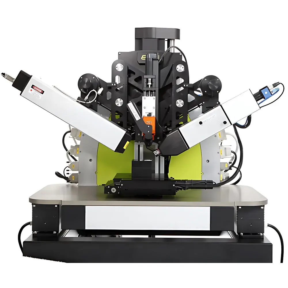
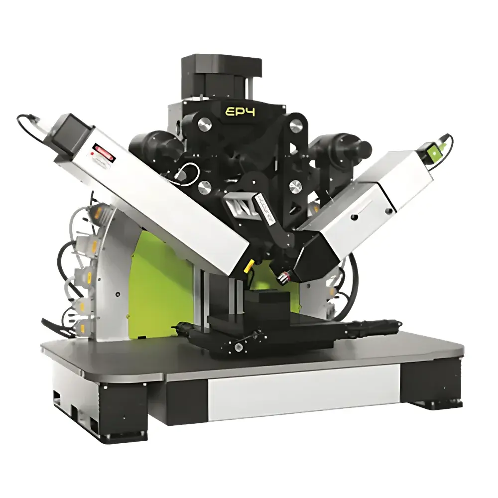
Accurion Nanofilm_EP4 Imaging Ellipsometer
| Brand | Accurion |
|---|---|
| Origin | Germany |
| Model | Nanofilm_EP4 |
| Spectral Range | 190–2750 nm |
| Spot Size | 1 µm |
| Angle of Incidence | 38°–90° |
| Sample Diameter | 2–12 inches |
| Spectral Resolution | 0.1 nm |
| Thickness Measurement Accuracy | 0.1 nm |
| Thickness Repeatability | 0.01 nm |
Overview
The Accurion Nanofilm_EP4 Imaging Ellipsometer is a high-precision, modular optical metrology platform engineered for nanoscale thin-film and interfacial characterization at microstructural resolution. Operating on the fundamental principles of spectroscopic ellipsometry—measuring the change in polarization state (Δ and Ψ) of light upon reflection from a sample surface—the Nanofilm_EP4 integrates real-time optical microscopy with automated nulling ellipsometry to deliver spatially resolved, quantitative film property mapping. Unlike conventional spot-based ellipsometers, the EP4 employs full-field imaging optics combined with a motorized, precision goniometric stage to maintain rigorous angular control across the entire field of view. Its 1 µm lateral resolution enables sub-micron feature analysis on heterogeneous surfaces, making it uniquely suited for characterizing patterned substrates, microfluidic interfaces, self-assembled monolayers (SAMs), and dynamic interfacial processes such as protein adsorption or Langmuir film expansion in situ.
Key Features
- Sub-micron spatial resolution (≤1 µm spot size) enabled by integrated high-NA microscope optics and optimized illumination geometry
- Full spectral coverage from deep UV to near-infrared (190–2750 nm) with 0.1 nm step resolution for dispersion-corrected optical constant extraction
- Automated four-zone nulling ellipsometry technique—eliminates systematic polarization artifacts and ensures accurate Δ/Ψ measurement across the full 0°–90° range
- Full-frame focusing technology: compensates for the inherent line-focus limitation of oblique-incidence ellipsometry, enabling diffraction-limited focus across the entire imaging field without mechanical scanning
- Real-time ellipsometric contrast imaging: generates video-rate intensity-modulated maps reflecting local variations in thickness, refractive index, and absorption coefficient
- Region-of-interest (ROI) analysis: supports user-defined polygonal or rectangular selection for localized spectroscopic ellipsometry and statistical parameter extraction
- Multi-region parallel analysis: acquires and processes ellipsometric data from up to 16 independent areas simultaneously
- Beam-cutting optics: suppresses substrate back-reflection interference—critical for ultra-thin films on transparent substrates (e.g., SiO₂/Si, glass, sapphire)
Sample Compatibility & Compliance
The Nanofilm_EP4 accommodates wafers and planar substrates from 50 mm (2″) to 300 mm (12″) in diameter, with optional vacuum chuck or liquid cell integration. It is fully compatible with solid–liquid, liquid–liquid, gas–liquid, and gas–solid interfaces via dedicated modules—including flow cells, temperature-controlled stages (−20°C to +80°C), electrochemical cells, and surface plasmon resonance (SPR) couplers. The system adheres to ISO/IEC 17025 calibration traceability requirements for optical metrology instruments. All hardware and software components are designed to support GLP/GMP-compliant environments, including audit-trail-enabled operation logs, user access controls, and electronic signature readiness per FDA 21 CFR Part 11 when paired with optional compliance software packages.
Software & Data Management
Control and analysis are performed via Accurion’s proprietary Nanofilm Analysis Suite v5.x—a Windows-based application built on a modular architecture supporting scriptable workflows, batch processing, and third-party API integration (Python, MATLAB). Raw ellipsometric data (Δ, Ψ, intensity) are stored in HDF5 format with embedded metadata (angle, wavelength, ROI coordinates, environmental conditions). The software includes physics-based regression modeling engines for multi-layer optical stack fitting (e.g., Cauchy, Tauc-Lorentz, Cody-Lorentz dispersion models), real-time fitting convergence monitoring, and uncertainty propagation reporting. Export options include CSV, ASCII, TIFF (for image overlays), and industry-standard formats compatible with OriginLab, Igor Pro, and JMP. Data integrity is enforced through checksum verification, versioned project files, and optional networked database archiving.
Applications
- In-situ monitoring of SAM formation kinetics, lipid bilayer assembly, and polymer brush swelling at air–water or solid–liquid interfaces
- Quantitative thickness and optical dispersion mapping of ALD/CVD-deposited dielectric stacks on patterned semiconductor wafers
- Correlative analysis of surface topography (via AFM co-registration) and optical anisotropy in 2D materials (MoS₂, graphene oxide)
- Real-time tracking of protein–ligand binding events on functionalized sensor surfaces using SPR–ellipsometry hybrid mode
- Microscale defect identification in anti-reflective coatings, OLED encapsulation layers, and photonic crystal slabs
- Dynamic interfacial rheology studies in microfluidic channels using synchronized flow control and time-resolved ellipsometric imaging
FAQ
What optical models are supported for multilayer fitting?
The Nanofilm Analysis Suite includes built-in dispersion models for amorphous silicon, silicon dioxide, silicon nitride, metals (Drude), organic polymers (Cauchy), and custom user-defined models via scripting interface.
Can the system operate under ambient, inert, or liquid environments?
Yes—standard configurations support ambient air and nitrogen purge; optional modules enable sealed liquid cells, electrochemical flow cells, and temperature-controlled chambers with optical access.
Is the instrument compatible with existing cleanroom infrastructure?
The Nanofilm_EP4 meets SEMI S2–0201 safety standards and features ESD-safe housing, vibration-damped optical baseplate, and Class 1000-compatible footprint; wafer handling accessories support SMIF pod integration.
How is calibration maintained over long-term operation?
Factory calibration is traceable to NIST standards; users perform routine verification using certified reference samples (Si/SiO₂ wafers, fused silica standards); automated alignment routines recalibrate optical path stability before each session.


