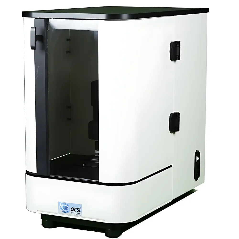
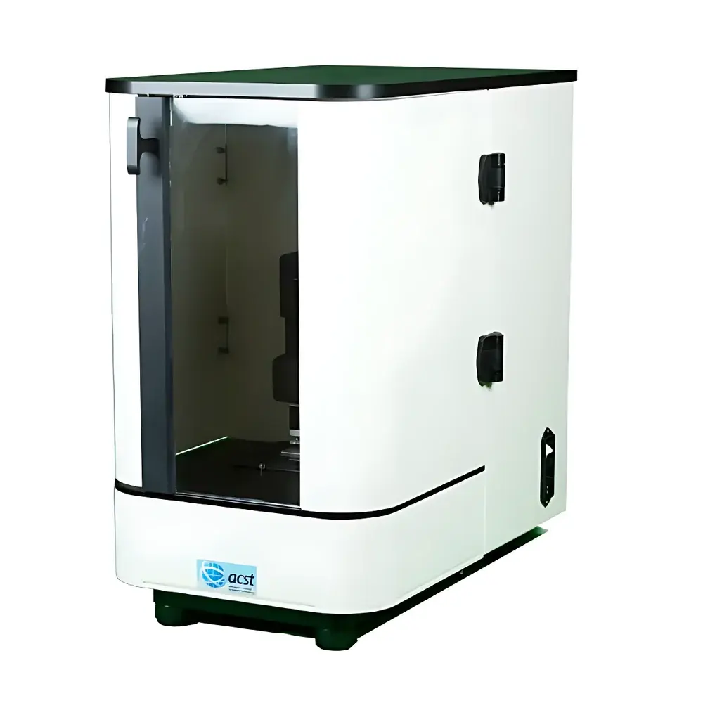
ACST NanoFab Desktop Micro- and Nanofabrication System
| Brand | ACST |
|---|---|
| Origin | USA |
| Manufacturer Type | Authorized Distributor |
| Import Status | Imported |
| Model | NanoFab |
| Price | USD 200,000 |
| Instrument Category | Microarray Fabrication System |
| Substrate Material | Silicon |
| Substrate Dimensions | 2 cm × 2 cm |
| Feature Size | 5 µm |
| Probe Anchoring Method | Atomic Stamp (Soft Lithography-Based) |
| Compatible Sample Types | Nucleic Acids, Proteins |
Overview
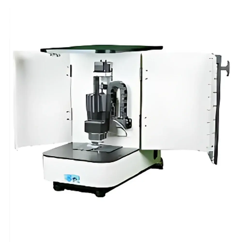
The ACST NanoFab Desktop Micro- and Nanofabrication System is a modular, benchtop platform engineered for precision surface patterning and functionalization at micro- and nanoscale resolutions. It integrates three complementary bottom-up and top-down fabrication modalities—microcontact printing (μCP), ultraviolet (UV) photolithography, and ultraviolet nanoimprint lithography (UV-NIL)—within a single, compact architecture. Unlike conventional scanning probe or vacuum-based nanofabrication tools, the NanoFab operates under ambient atmospheric conditions without requiring high-vacuum chambers, cryogenic stages, or complex beam alignment. Its core functionality relies on controlled molecular transfer (μCP), optical pattern projection (UV photolithography), and mechanical deformation of UV-curable resist (UV-NIL), enabling reproducible feature definition down to 5 µm with sub-nanometer Z-axis repeatability in height profiling. Designed for educational rigor and research-grade validation, the system supports iterative process development in semiconductor-compatible cleanroom-adjacent environments and teaching laboratories alike.
Key Features
- Triple-mode fabrication capability: seamless switching between μCP, UV photolithography, and UV-NIL workflows
- Ambient-condition operation—no vacuum pumps, inert gas purging, or thermal stabilization required
- Integrated atomic stamp module with PDMS and polyurethane elastomer compatibility for high-fidelity molecular transfer
- UV exposure unit with broadband 365 nm source and adjustable mask-to-substrate gap control (0–100 µm)
- UV-NIL stage with programmable force control (0.1–5 N), temperature regulation (25–90 °C), and real-time UV dose monitoring
- Real-time laser spot auto-centering system using quadrant photodiode feedback—eliminates periodic optical recalibration
- One-click scan automation: intelligent parameter prediction for cantilever engagement, force curve acquisition, and raster scanning
- Modular mechanical and electronic architecture—interchangeable modules share common drivers, controllers, and data buses
Sample Compatibility & Compliance
The NanoFab accommodates silicon wafers (2 cm × 2 cm), glass slides, gold-coated substrates, and polymer films compatible with standard microfabrication protocols. It supports direct immobilization of nucleic acids (e.g., DNA oligonucleotides, cDNA), proteins (antibodies, enzymes, receptors), and small-molecule ligands via thiol-gold, silane-oxide, or NHS-ester chemistries. All fabrication processes comply with ISO 14644-1 Class 5–7 cleanroom operational guidelines when used in controlled environments. The UV exposure subsystem meets IEC 62471 photobiological safety standards for UV-A radiation. Data acquisition and instrument control adhere to ALCOA+ principles (Attributable, Legible, Contemporaneous, Original, Accurate, Complete, Consistent, Enduring, Available), supporting GLP and GMP-aligned documentation workflows where required.
Software & Data Management
The PSX Control Suite provides a unified interface for hardware orchestration, protocol scripting, and image analysis. It includes preconfigured templates for μCP stamp alignment, photomask registration, NIL mold loading, and resist development timing. Scan data is stored in vendor-neutral HDF5 format with embedded metadata (timestamp, operator ID, substrate lot, process parameters). Built-in library management enables hierarchical organization, version tagging, and batch export to CSV, TIFF, or STS (Standard Test Specimen) formats. Audit trails record all user actions—including parameter changes, calibration events, and file exports—in accordance with FDA 21 CFR Part 11 requirements when configured with electronic signature modules. Remote monitoring and script-based automation are supported via Python API integration.
Applications
- Microcontact Printing (μCP): Fabrication of protein microarrays for immunoassay development; cell-adhesive peptide patterns for mechanobiology studies; conductive polymer stamps for flexible electronics prototyping
- UV Photolithography: Rapid prototyping of microfluidic channel masters; fabrication of electrode arrays for electrochemical biosensors; patterning of photoresist for subsequent RIE etching of Si or SiO₂
- UV Nanoimprint Lithography: High-throughput replication of plasmonic nanostructures for LSPR sensing; fabrication of anti-reflective moth-eye textures on optical substrates; creation of nanotopographic cues for stem cell differentiation assays
- Educational Use: Hands-on training in semiconductor process flow (spin-coating → UV exposure → development → etch → lift-off); comparative study of resolution limits across lithographic techniques; interdisciplinary labs bridging materials science, bioengineering, and device physics
FAQ
Is vacuum required for any NanoFab operation?
No. All three fabrication modes—μCP, UV photolithography, and UV-NIL—operate under ambient atmospheric conditions.
What substrate thicknesses are supported?
Standard 500 µm silicon wafers are optimal; substrates ranging from 100 µm to 1 mm thickness can be accommodated with optional stage adapters.
Can the system be integrated into existing cleanroom infrastructure?
Yes. The NanoFab meets SEMI S2-0201 safety standards and has been validated for use in ISO Class 5–7 environments with standard HEPA filtration.
Does the PSX software support automated batch processing?
Yes. Scripted workflows allow unattended execution of multi-step protocols across up to 12 substrates per session, with error logging and pause/resume capability.
Are calibration certificates traceable to NIST standards?
Dimensional calibration artifacts (e.g., NIST-traceable step-height standards) are included with each system shipment, and annual recalibration services are available through ACST-certified service centers.


