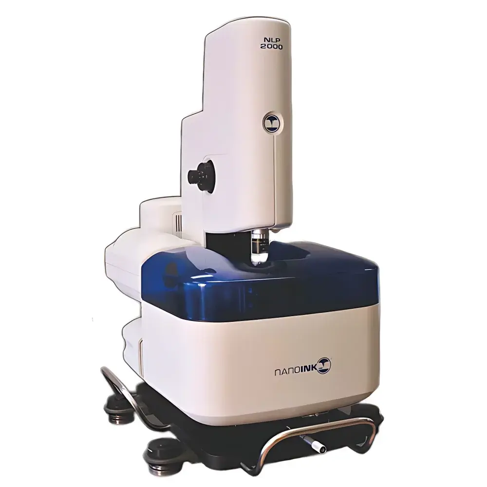
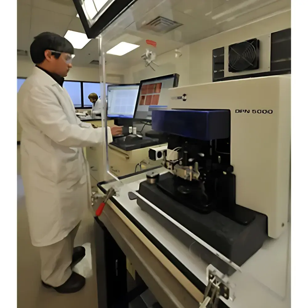
ACST NLP-2000 Dip-Pen Nanolithography Microarray Printing System
| Brand | ACST |
|---|---|
| Origin | USA |
| Manufacturer Type | Authorized Distributor |
| Product Category | Imported Instrument |
| Model | NLP-2000 |
| Price | USD 200,000 |
| Instrument Type | Microarray Chip System |
| Footprint | 4 cm × 4 cm × ~18 cm (H) |
| Substrate Compatibility | Silicon, SiO₂, Silanized Glass, Amine-Activated Slides, Metals, PDMS, Hydrogels, Polystyrene, Catalysts, Thiols |
| Minimum Feature Size | 10 nm |
| Patterning Method | Direct-Write Dip-Pen Nanolithography (DPN) |
| Printable Materials | Proteins, DNA/RNA, Antigens, Liposomes, Nanoparticles, Polyethylene Glycol (PEG), UV-Curable Polymers, Thermoset Polymers, Glycerol, Silanes |
| Viscosity Range | 1–20,000 cP |
| Print Area | 40 mm × 40 mm |
| Resolution | Sub-100 nm lateral, <5 nm height control |
| Probe Array Configurations | Single-tip to M-type multi-tip (up to 128 tips) |
| Environmental Control | Integrated Humidity & Temperature Chamber (±0.1 °C, ±2% RH) |
| Motion Stages | Piezoelectric XYZ linear stages + dual-axis goniometer (Tx/Ty) |
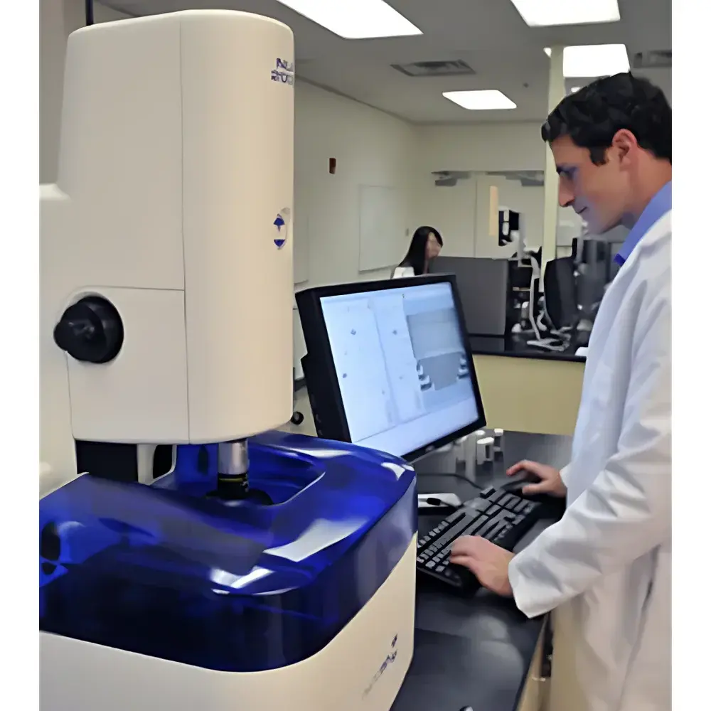
| Imaging | High-resolution optical microscope (10×–100×, 0.7 µm resolution) |
| Software | ACST NanoPattern Suite v4.2 (Scriptable, GLP-compliant audit trail, FDA 21 CFR Part 11 optional) |
Overview
The ACST NLP-2000 Dip-Pen Nanolithography Microarray Printing System is a benchtop, direct-write nanofabrication platform engineered for sub-100 nm precision deposition of molecular and polymeric “inks” onto diverse solid substrates. Based on the foundational Dip-Pen Nanolithography (DPN) technique pioneered by Prof. Chad Mirkin’s group at Northwestern University, the NLP-2000 implements a controlled, ambient-pressure, solvent-mediated mass transport mechanism—where molecular or colloidal inks are transported from an AFM-like cantilever tip across a meniscus bridge to the substrate surface. Unlike top-down lithographic methods requiring vacuum, plasma, or high-energy radiation, DPN operates under standard laboratory conditions (20–25 °C, 30–60% RH), preserving biomolecular integrity and enabling functional biochip fabrication without denaturation, shear stress, or UV-induced damage. The system integrates MEMS-fabricated probe arrays, closed-loop piezoelectric motion control, real-time optical monitoring, and programmable environmental regulation—making it uniquely suited for iterative, low-volume, high-fidelity microarray development in proteomics, diagnostics, nanomaterials engineering, and cell-microenvironment studies.
Key Features
- Sub-100 nm feature resolution with <5 nm height repeatability, validated via in situ optical imaging and post-process AFM/SEM correlation
- Multi-tip DPN array capability (M-type configuration supports up to 128 parallel pens), enabling high-throughput patterning of heterogeneous biomolecular libraries
- 40 mm × 40 mm motorized XY stage with active auto-leveling and dual-axis goniometric compensation (Tx/Ty), ensuring uniform tip–substrate contact across large-area substrates
- Integrated environmental chamber with independent temperature (±0.1 °C) and relative humidity (±2% RH) control, logged with timestamped metadata for GLP/GMP traceability
- Optical microscopy subsystem (10×–100× objectives, 0.7 µm resolution) co-registered with print coordinates for real-time process verification and defect mapping
- Viscosity-agnostic ink delivery: compatible with liquids ranging from 1 cP (aqueous buffers) to 20,000 cP (viscoelastic hydrogels and prepolymers)
- ACST NanoPattern Suite v4.2 software with Python scripting API, automated pattern sequencing, calibration workflow, and optional 21 CFR Part 11 compliance modules (electronic signatures, audit trail, user role management)
Sample Compatibility & Compliance
The NLP-2000 accepts a broad spectrum of printable materials—including native proteins, single-stranded/double-stranded DNA/RNA, antibodies, antigens, liposomes, metallic nanoparticles, PEG-based hydrogels, UV- and thermally curable polymers, silanes, and thiol-based monolayers—without chemical modification or derivatization. Compatible substrates include silicon wafers, fused silica, amine-functionalized glass slides, gold-coated surfaces, PDMS elastomers, polystyrene cultureware, catalyst-loaded membranes, and porous hydrogel matrices. All hardware and firmware comply with IEC 61000-6-3 (EMC emissions) and IEC 61000-6-2 (immunity). Software architecture supports ISO/IEC 17025-aligned data integrity protocols; optional validation packages include IQ/OQ documentation templates aligned with ASTM E2500 and USP Analytical Instrument Qualification guidelines.
Software & Data Management
The ACST NanoPattern Suite provides a unified interface for design import (SVG, DXF, GDSII), path optimization, probe assignment, environmental parameter scheduling, and real-time print supervision. Each print session generates a structured metadata file containing timestamp, environmental logs, stage position history, ink lot IDs, operator credentials, and checksum-verified image snapshots. Raw data files adhere to HDF5 format with embedded schema definitions (NIEM-compliant), facilitating integration into LIMS environments and FAIR-compliant repositories. Audit trails meet FDA 21 CFR Part 11 requirements when enabled, including biometric login options, electronic signature capture, and immutable record retention policies. Batch export supports CSV, TIFF, and OME-TIFF standards for downstream analysis in ImageJ/Fiji, MATLAB, or commercial bioinformatics platforms.
Applications
- Functionalized Biochips: Fabrication of multiplexed protein/DNA microarrays with attomole-level sensitivity and minimal cross-reactivity, supporting immunoassay development and biomarker discovery
- Nanoscale Sensor Functionalization: Site-specific immobilization of receptors, enzymes, or aptamers onto microelectrodes, SPR chips, and cantilever biosensors
- Cell-Material Interaction Studies: Patterning of extracellular matrix proteins (e.g., fibronectin, laminin) or synthetic peptides at subcellular resolution to direct stem cell adhesion, polarization, and differentiation
- Microfluidic Device Prototyping: Direct deposition of valves, hydrophobic barriers, or catalytic zones within PDMS channels without masking or etching steps
- Nanomaterial Assembly Templates: Guided nucleation of carbon nanotubes, graphene electrodes, or plasmonic nanostructures using chemically patterned SAMs
- Regenerative Medicine Scaffolds: Spatially resolved deposition of bioactive hydrogel precursors followed by two-photon or UV polymerization to generate 3D tissue-mimetic architectures
FAQ
What is the smallest printable feature size achievable with the NLP-2000?
The system achieves consistent 10 nm minimum linewidth under optimized humidity and dwell-time conditions; typical operational range spans 50 nm to 10 µm depending on ink rheology and substrate chemistry.
Can the NLP-2000 deposit multiple materials simultaneously?
Yes—using M-type multi-probe arrays, each pen can be loaded with a distinct ink formulation, enabling parallel, register-accurate co-patterning of proteins, nucleic acids, and nanoparticles in a single run.
Is the system compatible with sterile or biosafety-level 2 (BSL-2) workflows?
All fluidic components contacting inks are autoclavable or disposable; the environmental chamber supports HEPA-filtered air purge mode and can be integrated with laminar flow hoods per ISO 14644-1 Class 5 specifications.
Does ACST provide application support and method development assistance?
Yes—ACST offers on-site installation qualification, hands-on operator training, and collaborative application development through its NanoFabrication Support Center, including protocol optimization for novel ink–substrate combinations.
What maintenance is required for long-term stability?
Routine maintenance includes quarterly calibration of piezo stages, biannual replacement of consumable probe arrays and reservoir seals, and annual certification of environmental sensor accuracy against NIST-traceable standards.