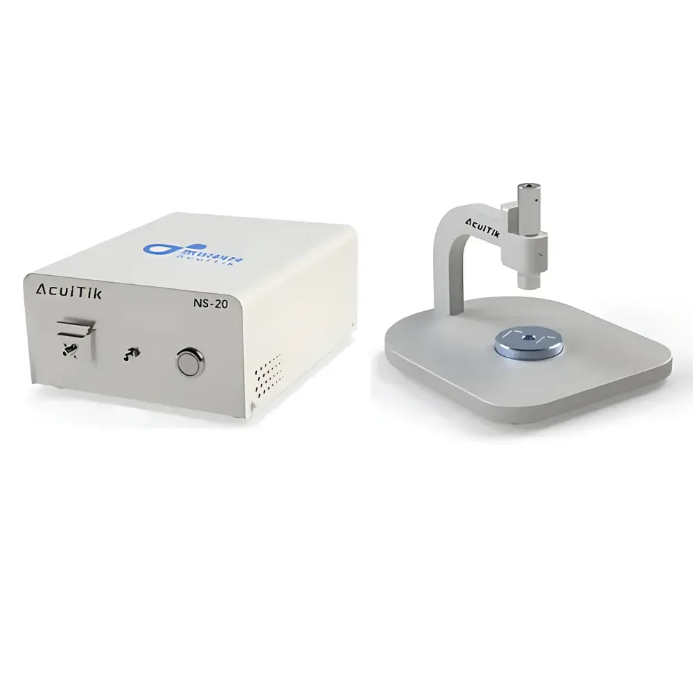
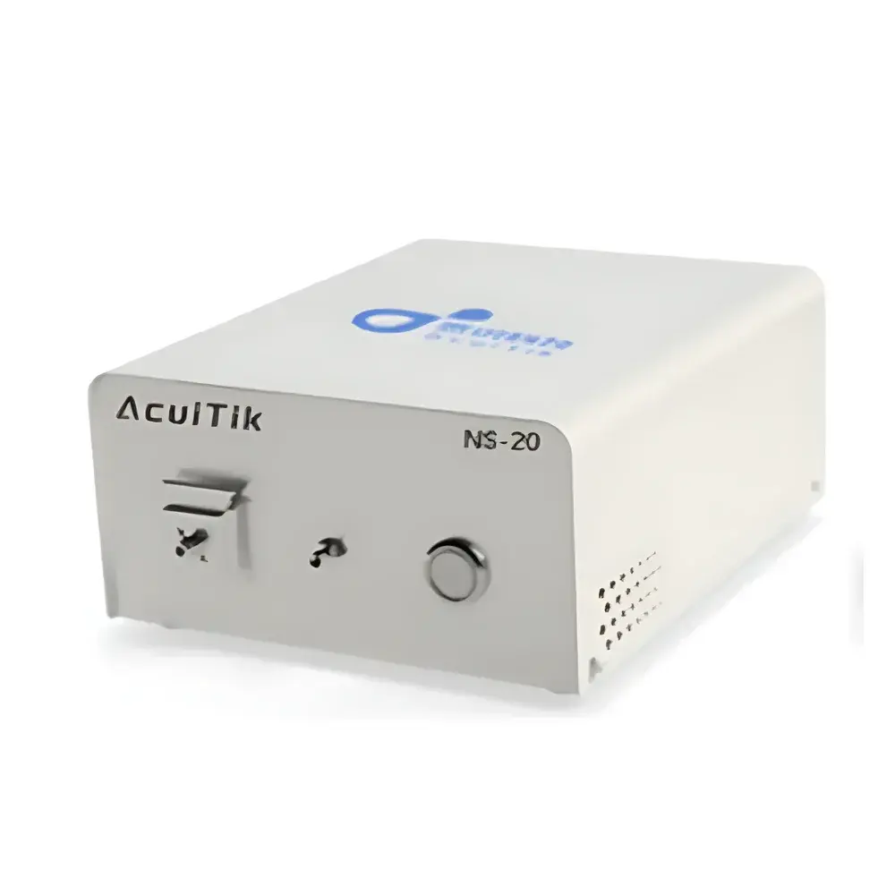
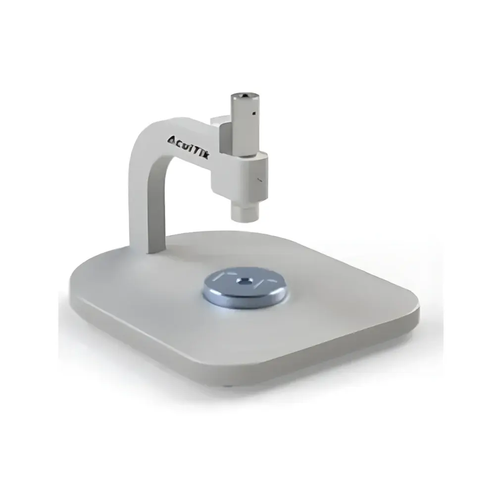
AcuiTik NS-20 Desktop Manual White Light Interferometric Thin-Film Thickness Metrology System
| Brand | AcuiTik |
|---|---|
| Origin | Shanghai, China |
| Manufacturer Type | Direct Manufacturer |
| Country of Origin | China |
| Model | NS-20 |
| Price Range | USD 7,000 – 35,000 |
| Wavelength Range | 190–1700 nm (configurable UV/VIS/NIR variants) |
| Thickness Measurement Range | 1 nm – 250 µm (dependent on optical configuration) |
| Accuracy | ±1 nm or ±0.2% (UV variant) |
| Precision (repeatability) | 0.02 nm (UV/VIS), 0.1 nm (NIR) |
| Stability (8-hour drift) | ≤0.05 nm (UV/VIS), ≤0.12 nm (NIR) |
| Spot Size | 1.5 mm diameter |
| Measurement Speed | <1 s per single-point acquisition |
| Light Source | Tungsten-halogen + Deuterium lamp (UV), Tungsten-halogen only (VIS/NIR) |
| Sample Diameter Compatibility | 1 mm – 300 mm (custom larger stages available) |
Overview
The AcuiTik NS-20 is a compact, manually operated desktop metrology system engineered for non-contact, high-resolution thin-film thickness measurement using white light interferometry (WLI). Based on the principle of spectral-domain interference, the instrument directs broadband collimated light vertically onto the sample surface; interference fringes generated at each dielectric interface are captured by a high-sensitivity spectrometer and processed via proprietary inverse modeling algorithms. This enables quantitative extraction of layer thickness, refractive index (n), and extinction coefficient (k) for single-layer and multilayer transparent or semi-transparent films—ranging from atomic-scale monolayers (≥1 nm) to thick polymer or oxide stacks (up to 250 µm). Designed for R&D laboratories, QC environments, and pilot-line process development, the NS-20 delivers sub-nanometer resolution without vacuum requirements, mechanical contact, or destructive sampling—making it ideal for fragile substrates (e.g., OLED anodes, photoresist-coated wafers, biomedical coatings) and soft materials (e.g., hydrogels, spin-cast polymers).
Key Features
- Full domestic R&D and manufacturing: 100% indigenously developed hardware architecture and core optical engine—ensuring supply chain autonomy and long-term serviceability.
- Configurable spectral modules: Three factory-tuned variants—NS-20 UV (190–1100 nm), NS-20 VIS (380–1050 nm), and NS-20 NIR (950–1700 nm)—optimized for specific material dispersion profiles and absorption edges.
- Sub-angstrom static stability: Achieves ≤0.05 nm 8-hour thermal drift (UV/VIS) through passive thermal mass design, low-noise electronics, and vibration-damped optical bench integration.
- Multi-layer inversion capability: Solves for ≥5-layer stack parameters simultaneously using constrained Levenberg-Marquardt optimization with physically bounded n/k dispersion models (Cauchy, Sellmeier, Tauc-Lorentz).
- One-click measurement workflow: PolarX software automates spectral acquisition, baseline correction, fringe envelope detection, and model convergence—reducing operator dependency and training time.
- Modular mechanical design: Includes optional large-stage adapter (up to Ø300 mm), portable carry case with shock-absorbing foam, and manual XYZ translation stage with 0.1 µm vernier readout.
Sample Compatibility & Compliance
The NS-20 accommodates diverse substrate geometries—from micro-patterned silicon wafers (Ø1–150 mm) to curved glass lenses, flexible PET foils, and irregularly shaped optoelectronic components. Its non-contact operation eliminates risk of scratching delicate anti-reflective coatings, organic semiconductor layers, or nanoimprinted structures. The system supports ISO 9001-aligned calibration traceability via NIST-traceable SiO₂/Si reference standards. While not certified for GMP production release, its audit-ready data logging (timestamped spectra, raw interferograms, fit residuals) and user-accessible parameter history meet GLP documentation requirements for academic and industrial R&D reporting. All firmware and PolarX software comply with IEC 62304 Class B for medical device-related development workflows.
Software & Data Management
PolarX—a native Windows application built on Qt/C++—provides full control over acquisition parameters (integration time, averaging count, spectral binning), real-time spectrum visualization, and iterative optical modeling. Key modules include: (1) Recipe Manager for saving multi-layer stack definitions and measurement presets; (2) Formulation Validator for comparing measured n/k against theoretical databases (e.g., Palik, SOPRA); (3) Batch Analyzer for automated throughput of wafer maps (via optional motorized stage); and (4) Export Engine supporting ASTM E2919-compliant CSV, HDF5, and PDF report generation. Audit trails record all user actions, parameter changes, and software version metadata—enabling compliance with FDA 21 CFR Part 11 when deployed with Windows domain authentication and electronic signature protocols.
Applications
- Semiconductor front-end: Monitoring ALD/PECVD-deposited SiNₓ, HfO₂, and Ta₂O₅ gate dielectrics on 200 mm/300 mm wafers.
- Display manufacturing: Measuring ITO, MoO₃, and NiOₓ hole transport layers in perovskite and QLED prototypes.
- Optical coating QA: Verifying quarter-wave stacks in AR/HR filters and laser cavity mirrors.
- Biomedical thin films: Quantifying chitosan, PLLA, or PEG-based drug-eluting coatings on stents and microfluidic channels.
- Photovoltaics R&D: Characterizing tandem cell interlayers (e.g., SnO₂/EVA/Perovskite/CuSCN) without cross-contamination.
- Academic surface science: In-situ monitoring of self-assembled monolayers (SAMs) and Langmuir-Blodgett films during deposition.
FAQ
What film transparency requirements apply for reliable WLI measurement?
WLI requires measurable reflectance contrast between adjacent layers. Films with absorption coefficients α > 10⁵ cm⁻¹ (e.g., thick metals, carbon black composites) yield weak or absent interference fringes. Semi-transparent oxides, nitrides, polymers, and organic semiconductors are fully supported.
Can the NS-20 measure rough or patterned surfaces?
Yes—within limits. Surface RMS roughness should be <10% of the optical wavelength used (e.g., <50 nm for 500 nm center wavelength). For structured surfaces (e.g., gratings), spot size must exceed feature period by ≥3× to avoid diffraction-induced spectral distortion.
Is calibration required before each measurement session?
No. Factory calibration is stable for ≥12 months under controlled lab conditions (23±2°C, <50% RH). Daily verification using a supplied SiO₂-on-Si standard is recommended for critical applications.
Does PolarX support scripting or API integration?
Yes. PolarX exposes a COM interface for MATLAB, Python (pywin32), and LabVIEW integration—enabling automated test sequences, custom fitting routines, and MES/SCADA data ingestion.
What maintenance does the NS-20 require?
Annual spectrometer wavelength recalibration and optical path cleaning (per ISO 10110-7). No consumables or gas supplies are needed. All optics are sealed and humidity-resistant.


