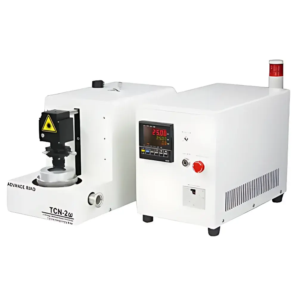
ADVANCE RIKO TCN-2ω Nanoscale Thin-Film Thermal Conductivity Measurement System
| Brand | ADVANCE RIKO |
|---|---|
| Origin | Japan |
| Model | TCN-2ω |
| Measurement Principle | 2ω Lock-in Thermography (Frequency-Domain Modulated Joule Heating) |
| Test Temperature | Ambient (23 ± 2 °C) |
| Sample Dimensions | 10–20 mm (L) × 10 mm (W) × 0.3–1 mm (total thickness, including substrate) |
| Substrate Materials | Si (recommended), Ge, Al₂O₃ |
| Metal Transducer Film | Au (100 nm, 1.7 mm × 15 mm) |
| Thermal Conductivity Range | 0.1–10 W·m⁻¹·K⁻¹ |
| Atmosphere | Ambient air |
| Compliance | ISO/IEC 17025-aligned methodology, compatible with GLP documentation workflows |
Overview
The ADVANCE RIKO TCN-2ω Nanoscale Thin-Film Thermal Conductivity Measurement System is a purpose-built, turnkey instrument engineered for the quantitative determination of through-plane (cross-sectional) thermal conductivity (λ⊥) of nanoscale thin films — typically 10–100 nm in thickness — deposited on thermally conductive substrates. It implements the well-established 2ω (two-omega) frequency-domain photothermal technique, wherein a sinusoidally modulated electrical current (frequency f) is applied to a metallic transducer layer (e.g., 100 nm Au), inducing periodic Joule heating at frequency f. Due to quadratic dependence of resistive power dissipation on current, the resulting thermal oscillation occurs at twice the excitation frequency (2f). The system precisely measures the in-phase (real) component of the surface temperature oscillation via lock-in detection of thermoreflectance signals from the same metal film. This signal is directly related to the thermal diffusivity and conductivity of the underlying film under a one-dimensional heat conduction model, assuming negligible lateral heat spreading and dominant vertical heat flow into the substrate. The TCN-2ω eliminates reliance on complex optical alignment or vacuum environments, delivering reproducible λ⊥ values without requiring lithographic patterning or microfabrication infrastructure — making it suitable for routine metrology in materials development labs, semiconductor process R&D, and thermoelectric thin-film characterization.
Key Features
- Direct, non-contact measurement of cross-plane thermal conductivity for films between 10 nm and 100 nm thickness
- Integrated lock-in amplifier and high-sensitivity thermoreflectance detection optimized for Au transducer films
- No vacuum chamber required: fully operational under ambient atmospheric conditions
- Minimal sample preparation: sputter- or evaporate-deposited 100 nm Au strip (1.7 mm × 15 mm) serves as both heater and thermometer
- Validated one-dimensional thermal model incorporating substrate thermal effusivity (Si, Ge, Al₂O₃ supported)
- Traceable calibration protocol based on reference SiO₂-on-Si samples with independently verified λ⊥
- Engineered for stability: temperature-controlled stage (<±0.1 °C) and low-noise current source ensure measurement repeatability (RSD < 3% across replicate runs)
Sample Compatibility & Compliance
The TCN-2ω accommodates rigid planar samples with total thickness 0.3–1.0 mm, including substrate. Standard configurations use single-crystal silicon wafers (300–500 µm thick) as substrates due to their uniform thermal properties and widespread availability; alternative high-effusivity substrates such as germanium and sapphire (Al₂O₃) are supported. The system is routinely used for low-k dielectrics (e.g., SiO₂, SiCN, porous organosilicates), organic semiconductors, transition metal dichalcogenides (TMDs), and thermoelectric thin films (e.g., Bi₂Te₃, Sb₂Te₃). All measurements adhere to principles aligned with ISO/IEC 17025 for testing laboratories, and raw data acquisition supports audit-ready documentation per GLP requirements. While not FDA-certified as a medical device, its data structure and metadata logging (timestamp, current amplitude, lock-in phase/gain, ambient T/P) satisfy baseline traceability expectations for QC/QA workflows in semiconductor and advanced packaging R&D.
Software & Data Management
The TCN-2ω operates via dedicated Windows-based control software that manages current source modulation, lock-in parameter tuning (time constant, filter slope), real-time signal visualization, and automated data export in CSV and HDF5 formats. Each measurement session logs full experimental metadata: excitation frequency (10 Hz–10 kHz range), RMS current amplitude, measured 2ω amplitude and phase, ambient temperature, and user-defined sample identifiers. Exported datasets include columnar headers compliant with ASTM E2986-22 (Standard Practice for Reporting Thermal Property Data) conventions. The software supports batch processing of multiple samples and includes built-in curve-fitting routines for extracting λ⊥ using the published analytical solution for the three-layer (metal/film/substrate) thermal stack. Audit trails are retained locally; no cloud upload or telemetry is enabled by default — ensuring full data sovereignty.
Applications
- Thermal interface material (TIM) development: quantifying λ⊥ of polymer-nanocomposite thin films for flip-chip and 3D IC packaging
- Low-k interlayer dielectric qualification: correlation of porosity, density, and cross-plane λ in BEOL integration stacks
- Thermoelectric thin-film optimization: decoupling electronic and lattice contributions via λ⊥ vs. σ and S measurements
- Fundamental phonon transport studies in 2D materials (MoS₂, h-BN) grown by CVD or exfoliation
- Process monitoring of ALD/CVD-grown oxide/nitride layers in pilot-line fabrication environments
FAQ
What substrate materials are recommended for optimal accuracy?
Silicon is strongly recommended due to its well-characterized thermal effusivity (~1.6 × 10⁶ W·s⁰·⁵·m⁻²·K⁻¹), mechanical rigidity, and minimal interfacial thermal resistance with common dielectric films. Germanium and Al₂O₃ may be used when higher substrate effusivity is needed to enhance signal-to-noise ratio for ultra-low-λ films (<0.5 W·m⁻¹·K⁻¹).
Can the system measure films on flexible or transparent substrates?
No. The TCN-2ω requires rigid, thermally massive substrates capable of acting as an effective heat sink. Polymeric, glass, or PET substrates introduce significant lateral heat loss and violate the 1D conduction assumption; they are incompatible with the core measurement model.
Is calibration required before each measurement?
A one-time system sensitivity calibration is performed during installation using a certified SiO₂-on-Si reference sample. Subsequent measurements rely on this fixed calibration factor; no daily recalibration is necessary unless hardware configuration changes.
How does the TCN-2ω handle interfacial thermal resistance (Kapitza resistance)?
The standard analysis assumes negligible interfacial resistance between film and substrate. For cases where RK is suspected to dominate (e.g., weakly bonded organic films), users may apply iterative fitting incorporating an additional thermal boundary resistance term — though this requires independent estimation or complementary TDTR validation.
Does the software support automated report generation for regulatory submissions?
Yes. The software exports structured data files compatible with LIMS integration and allows user-defined templates for PDF report generation, including instrument ID, operator name, date/time stamp, and measurement uncertainty estimates derived from repeated measurements per ASTM E691 practice.
Related Products


