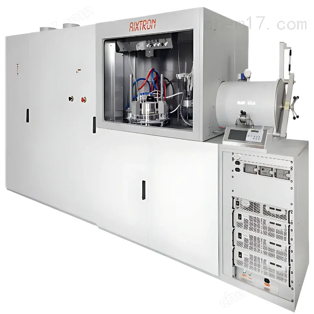
AIXTRON G10 Metal-Organic Chemical Vapor Deposition (MOCVD) System
| Brand | AIXTRON |
|---|---|
| Origin | Germany |
| Model | G10 |
| Heating Method | Hot-Wall |
| Substrate Sizes | 3×2 inch, 1×4 inch, 1×3 inch, 1×2 inch (carrier exchange supports 6×2 inch, 3×3 inch, 1×6 inch) |
| Ga₂O₃ Growth Rate | >3 µm/h |
| Ga₂O₃ Surface Roughness (5 µm × 5 µm, AFM on Ga₂O₃ substrate) | ≤1.0 nm |
| Temperature Control | Triple-zone tungsten filament heating, up to 1400 °C |
| Showerhead-to-Substrate Spacing | Adjustable from 5 mm to 25 mm |
| In-situ Monitoring | Real-time wafer surface temperature mapping and warp measurement |
| Application Domain | Semiconductor thin-film epitaxy |
| Film Types | Metallic and compound semiconductor layers (e.g., Ga₂O₃, GaN, InP, GaAs, InSb, GaInNAs, II–VI) |
Overview
The AIXTRON G10 Metal-Organic Chemical Vapor Deposition (MOCVD) system is a high-precision, hot-wall thermal CVD platform engineered for the controlled epitaxial growth of compound semiconductor and metallic thin films. It operates on the fundamental principle of metal-organic precursor pyrolysis: volatile organometallic compounds (e.g., TMGa, TEGa, DEZn) and hydride gases (e.g., NH₃, PH₃, AsH₃) are introduced into a heated reaction chamber via inert carrier gases (N₂ or H₂), where thermally activated decomposition and surface reactions yield stoichiometric, crystalline thin films on heated substrates. Designed for seamless scalability—from R&D prototyping to pilot-line production—the G10 supports heterogeneous substrate configurations including 3×2 inch, 1×4 inch, and 1×2 inch wafers, with carrier-exchange capability enabling flexible throughput for non-standard formats such as 6×2 inch or 3×3 inch arrays. Its triple-zone tungsten filament heating architecture delivers precise thermal uniformity up to 1400 °C, essential for high-quality Ga₂O₃, GaN, and InP heterostructures.
Key Features
- Hot-wall reactor design ensures superior thermal stability and reduced wall parasitic reactions compared to cold-wall configurations.
- Adjustable showerhead-to-substrate spacing (5–25 mm) enables fine-tuned gas-phase residence time and boundary layer control for improved film uniformity and conformality.
- In-situ, non-contact wafer temperature mapping via multi-point pyrometry provides real-time spatial thermal profiling across the entire substrate surface.
- Integrated wafer warp monitoring during growth allows dynamic feedback on thermal stress evolution—critical for minimizing defect generation in lattice-mismatched heteroepitaxy.
- Modular gas delivery system with mass flow controllers (MFCs) calibrated for organometallic precursors and corrosive hydrides, compliant with SEMI S2/S8 safety standards.
- Robust vacuum architecture featuring turbomolecular pumping and cryogenic trapping for high-purity process environments and low residual hydrocarbon contamination.
Sample Compatibility & Compliance
The G10 accommodates a broad range of substrate materials including sapphire, SiC, Si, GaN-on-Si, and native Ga₂O₃ wafers, with mechanical compatibility for both standard and custom cassette-based loading. It supports growth of III–V (GaN, InP, GaAs), IV–IV (SiGe), II–VI (ZnSe, CdTe), and ultra-wide-bandgap oxides (β-Ga₂O₃). The system meets ISO 14644-1 Class 5 cleanroom integration requirements and incorporates hardware-level interlocks aligned with IEC 61508 functional safety principles. Process documentation and audit trails comply with GLP and pre-GMP frameworks; optional 21 CFR Part 11-compliant software modules support regulated development workflows in photonics and power electronics qualification.
Software & Data Management
The system runs on AIXTRON’s proprietary ProcessControl™ software suite, offering recipe-driven operation with version-controlled parameter sets, automated ramp/soak profiles, and event-logged execution history. All temperature maps, MFC setpoints, pressure transients, and sensor diagnostics are timestamped and stored in SQLite-based local databases, exportable to CSV or HDF5 for traceability and statistical process control (SPC). Remote monitoring via secure TLS-encrypted web interface enables off-site engineering oversight without compromising data integrity. Integration with third-party MES platforms (e.g., CIM300, FactoryTalk) is supported through OPC UA server interfaces.
Applications
The G10 serves critical roles in the fabrication of high-electron-mobility transistors (HEMTs), laser diodes (LDs), vertical-cavity surface-emitting lasers (VCSELs), UV photodetectors, and RF power amplifiers. Its reproducible Ga₂O₃ growth (>3 µm/h at ≤1.0 nm RMS roughness over 5 µm × 5 µm) enables rapid development of normally-off power switches. For GaN-on-Si epiwafers, the system delivers low-dislocation-density templates suitable for 650 V+ devices. In academic and national lab settings, it facilitates combinatorial studies of ternary and quaternary alloys (e.g., GaInNAs, AlGaN) under precisely controlled V/III ratios and growth temperatures.
FAQ
What substrate sizes does the G10 support natively, and how is carrier exchange implemented?
The system accepts 3×2 inch, 1×4 inch, 1×3 inch, and 1×2 inch substrates using dedicated carriers; carrier exchange enables reconfiguration for 6×2 inch, 3×3 inch, or 1×6 inch arrangements without hardware modification.
Is real-time temperature mapping performed optically or via embedded sensors?
Temperature mapping is performed non-invasively using multi-wavelength pyrometry with spatial resolution down to 1 mm² across the full wafer diameter.
Does the G10 support in-situ spectroscopic monitoring (e.g., reflectance anisotropy or ellipsometry)?
The reactor flange includes standardized optical viewports (CF100 and CF63) compatible with third-party in-situ metrology tools; integration requires customer-supplied hardware and software synchronization.
What level of vacuum base pressure is achievable, and what pumping configuration is used?
Base pressure reaches ≤5×10⁻⁸ mbar using a dual-stage turbomolecular pump combined with liquid nitrogen-cooled cryopanels for hydrocarbon and water vapor capture.
Can the G10 be qualified for ISO 9001-certified manufacturing environments?
Yes—full FAT/SAT documentation, calibration certificates for all critical sensors (thermocouples, MFCs, pressure gauges), and IQ/OQ protocols are available upon request for quality system alignment.


