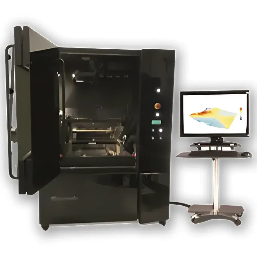
Akrometrix Thermal Warpage Measurement System
| Brand | Akrometrix |
|---|---|
| Origin | USA |
| Model | Customized |
| Sample Size Range | 0.5 mm × 0.5 mm to 400 mm × 400 mm |
| Warpage Resolution | <1 µm |
| Data Acquisition Density | 1.4 million points per 2 seconds |
| Temperature Control | IR heating + convection cooling |
| Temp Range | −50 °C to 300 °C |
| Reflow Simulation Support | up to 300 °C |
Overview
The Akrometrix Thermal Warpage Measurement System is a non-contact, high-speed optical metrology platform engineered for quantitative, real-time characterization of thermally induced dimensional changes in planar materials and assemblies. It operates on the principle of digital image correlation (DIC) combined with precision thermal actuation—capturing full-field surface displacement and deformation during controlled thermal ramping or dwell cycles. Unlike point-sensor-based methods (e.g., LVDTs or strain gauges), this system delivers spatially resolved warpage maps across the entire sample surface, enabling detection of localized curvature, gradient-driven bending, and anisotropic expansion behavior. Designed specifically for reliability engineering and process validation in microelectronics packaging, PCB manufacturing, and advanced composite development, it supports both R&D-grade material qualification and production-line process control under ISO/IEC 17025–aligned test environments.
Key Features
- Non-contact, full-field optical measurement using high-resolution CCD imaging and sub-pixel DIC algorithms
- Simultaneous acquisition of vertical displacement (Z-axis warpage), in-plane strain (εxx, εyy, γxy), and derived coefficients including coefficient of thermal expansion (CTE) and curvature radius
- Thermal chamber with dual-mode control: rapid infrared (IR) heating for steep ramp rates (up to 3.5 °C/s) and forced convection cooling for precise low-temperature stabilization (−50 °C to 300 °C)
- Scalable field-of-view accommodating samples from 0.5 mm × 0.5 mm microcomponents (e.g., die attach substrates) to large-format 400 mm × 400 mm panels (e.g., panel-level packaging or automotive composites)
- Real-time data throughput of 1.4 million measurement points per 2 seconds—enabling high-temporal-resolution tracking of transient warpage dynamics during reflow profiles
- Integrated calibration traceability to NIST-traceable standards for displacement and temperature; compliant with ASTM E2923 (Standard Practice for Quantitative Thermal Expansion Measurements) and IPC-9701A (Performance Test Methods for Surface Mount Solder Attachments)
Sample Compatibility & Compliance
The system accommodates rigid and semi-rigid planar specimens—including bare silicon wafers, molded plastic packages (QFN, BGA, LGA), laminated PCBs, metal-core boards, ceramic substrates, and fiber-reinforced polymer composites. Specimen mounting uses vacuum chucks or low-stress kinematic fixtures to minimize mechanical constraint artifacts. All thermal profiles—including JEDEC-standard reflow cycles (J-STD-020), thermal cycling (MIL-STD-883 Method 1010), and HALT-like extreme ramp protocols—are programmable and repeatable within ±0.3 °C accuracy. The platform meets requirements for GLP-compliant data integrity: audit trails, electronic signatures, and 21 CFR Part 11–ready software architecture are available as optional configurations.
Software & Data Management
Akrometrix Warpage Analysis Suite (WAS) provides a unified interface for test definition, live visualization, post-processing, and report generation. Raw DIC data is stored in HDF5 format with embedded metadata (timestamp, thermal setpoint, camera exposure, lens calibration). Built-in modules support automated warpage peak detection, contour mapping, CTE slope fitting over user-defined temperature intervals, and comparative analysis across multiple runs. Export options include CSV, MATLAB .mat, and PDF reports conforming to internal QA templates or external customer specifications (e.g., IATF 16949 PPAP submissions). Data archives are structured for long-term retention and version-controlled revision history per ISO 9001:2015 clause 7.5.3.
Applications
- Qualification of underfill, molding compound, and substrate CTE mismatch in flip-chip and fan-out wafer-level packaging
- Validation of solder joint reliability under thermal-mechanical stress in automotive ECUs and ADAS modules
- Process window development for reflow oven profiling and cold plate quenching in high-density interconnect assembly
- Material screening for low-warpage laminate selection in 5G mmWave antenna substrates
- Failure root cause analysis of popcorning, delamination, or solder bridging linked to out-of-plane distortion
- Supporting DOE studies for DOE-based optimization of mold temperature, hold time, and cool-down rate in injection-molded structural components
FAQ
What sample thicknesses can be measured?
The system measures surface deformation only; thickness is not a limiting factor, though optical access to both top and bottom surfaces is required for differential curvature analysis. Typical use cases range from 50 µm thin-film devices to 5 mm thick metal brackets.
Is vacuum chucking compatible with warpage-sensitive thin substrates?
Yes—customizable low-vacuum chucks with distributed pressure zones prevent localized buckling; optional soft-gasket interfaces are available for fragile or warped pre-test samples.
Can the system operate inside a cleanroom environment?
All models are rated for Class 1000 (ISO 6) cleanrooms; optional HEPA-filtered purge gas integration and static-dissipative enclosures are available upon request.
How is temperature uniformity validated across large-area samples?
Each system includes a calibrated multi-point thermocouple array (up to 16 channels) mounted on reference plates; uniformity mapping is performed per IQ/OQ protocol prior to delivery and annually during PQ maintenance.
Does the software support automated pass/fail criteria against industry standards?
Yes—WAS allows definition of zone-specific warpage thresholds (e.g., ≤25 µm at center, ≤15 µm at corners per IPC-9701A), with real-time flagging and statistical SPC charting integrated into export workflows.


