Allresist AR-N 4600 (Atlas 46) UV Negative Photoresist
| Brand | Allresist |
|---|---|
| Origin | Germany |
| Manufacturer Type | Authorized Distributor |
| Origin Category | Imported |
| Model | AR-N 4600 (Atlas 46) |
| Pricing | Available Upon Request |
Overview
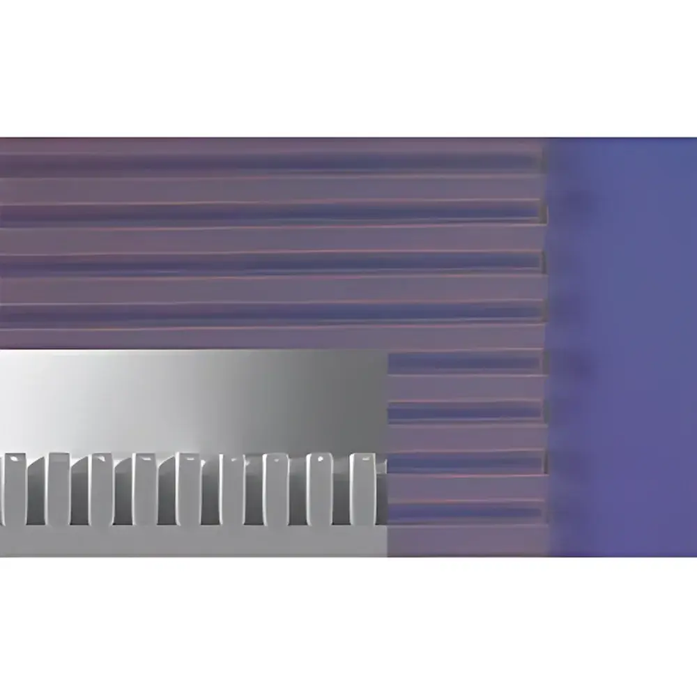
Allresist AR-N 4600 (Atlas 46) is a high-performance, solvent-based UV-negative photoresist engineered for demanding microfabrication processes in semiconductor, MEMS, and LIGA (Lithographie, Galvanoformung, Abformung) applications. Unlike conventional thin-film resists, AR-N 4600 is formulated to support thick-film lithography—enabling uniform, mechanically robust resist layers with thicknesses ranging from 10 µm (at 1000 rpm spin-coating) up to 200 µm under optimized process conditions. Its crosslinking mechanism relies on deep-UV (i-line, 365 nm) exposure followed by thermal post-exposure bake (PEB), resulting in highly insoluble, chemically resistant structures ideal for subsequent electroplating, reactive ion etching (RIE), or long-term structural retention.
Key Features
- Thick-film capability: Achieves consistent film thicknesses from 10 µm to >200 µm via spin-coating or spray-coating, with excellent edge definition and minimal stress-induced cracking.
- Two formulation variants: AR-N 4600-10 (SX) offers superior structural integrity and dimensional stability for permanent resist molds; AR-N 4650-10 (SX) provides enhanced developability and residue-free removal after electroforming, optimizing compatibility with Ni or Cu electroplating workflows.
- High resolution and aspect ratio: Supports sub-micron feature definition with aspect ratios exceeding 10:1 when patterned using contact or proximity aligners equipped with i-line illumination.
- Thermal and chemical robustness: Withstands temperatures up to 180 °C during PEB and exhibits resistance to common plating baths (e.g., Watts nickel, acid copper), organic solvents, and plasma etchants (CF4/O2, SF6).
- Process compatibility: Designed for integration into standard cleanroom photolithography lines—including HMDS adhesion promotion, soft/hard bake, UV exposure (365 nm), and aqueous alkaline development (e.g., Microposit 351 or TMAH-based developers).
Sample Compatibility & Compliance
AR-N 4600 demonstrates reliable adhesion across silicon wafers, glass substrates, metal-coated surfaces (e.g., Ti/Au, Cr/Ni), and ceramic carriers—especially when preceded by hexamethyldisilazane (HMDS) vapor priming. It complies with industry-standard fabrication protocols referenced in SEMI standards (SEMI D3–1107, SEMI F20–0218) and supports GLP/GMP-aligned documentation requirements when used in qualified production environments. While not classified as a medical device or FDA-regulated material, its trace metal content (<10 ppb Na, K, Fe, Cu) meets typical semiconductor-grade purity specifications. Batch-to-batch reproducibility is certified per ISO 9001 quality management systems maintained by Allresist GmbH.
Software & Data Management
As a consumable photoresist material—not an instrument—AR-N 4600 does not incorporate embedded firmware or software interfaces. However, its process parameters (spin speed, bake profiles, exposure dose, developer concentration/temperature) are fully compatible with industry-standard lithography data management platforms including LithoTrack™, YieldStar™, and open-source MES integrations (e.g., via SECS/GEM protocol). Process recipes can be archived, version-controlled, and audited in accordance with 21 CFR Part 11-compliant electronic record systems when deployed in regulated manufacturing settings. Certificate of Analysis (CoA), lot-specific spectral absorption data (UV-Vis), and viscosity reports are provided digitally with each shipment.
Applications
- LIGA-based fabrication of high-aspect-ratio microstructures for sensors, actuators, and RF components.
- MEMS packaging and cavity encapsulation requiring durable, hermetic resist molds.
- Electroplating masters for precision micro-metal parts in aerospace and medical device manufacturing.
- Maskless direct-write lithography (e.g., laser interference lithography) where thick, low-shrinkage resist layers are critical.
- Prototyping of microfluidic channel architectures and optical waveguide templates.
FAQ
What is the recommended exposure dose for AR-N 4600 under i-line illumination?
Typical exposure ranges from 150–300 mJ/cm² depending on film thickness and desired crosslink density; optimization requires empirical calibration using a calibrated radiometer.
Can AR-N 4600 be applied via spray coating instead of spin coating?
Yes—spray application enables uniform deposition on non-planar or large-area substrates; process parameters require adjustment for droplet size, nozzle distance, and solvent evaporation rate.
Is AR-N 4600 compatible with deep-UV (248 nm) or EUV exposure sources?
No—it is specifically formulated for i-line (365 nm) and broadband UV (300–450 nm); performance under shorter wavelengths is not characterized or guaranteed.
How should unused AR-N 4600 be stored to maintain shelf life?
Store unopened bottles at 2–8 °C in the dark; allow to equilibrate to room temperature before opening to prevent condensation; shelf life is 12 months from manufacture date when stored properly.
Does AR-N 4600 require a post-exposure bake (PEB)?
Yes—thermal PEB at 90–110 °C for 30–60 minutes is essential to complete crosslinking and maximize chemical resistance and mechanical stability.


